


so-logic |

"Als Geschäftsführer eines innovativen Unternehmens in Wien bin ich besonders stolz auf die große Zufriedenheit und das Vertrauen unserer internationalen Geschäftspartner. Diese positive Resonanz bestätigt unseren Anspruch auf höchste Qualität und bildet die Grundlage für die hohe Motivation des gesamten Teams."
Peter Thorwartl
So-logic ist spezialisiert auf Beratung, Entwicklung und Training für technische Programme, vor allem im Bereich der Nachrichtentechnik. Wir bietet viele Wege an, um Ihre Zeit zu sparen - von simpler Code-Durchsicht bis zu Turn-Key-Lösungen. So-logic besteht aus einem besonders hoch spezialisiertes Team, um Ihr Konzept zu realisieren.
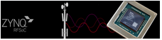
Unsere Erfahrung begann bereits mit den ersten FPGA-Entwicklungen.
Bereits mit den ersten kommerziell verfügbaren FPGA-Familien entwickelt das So-logic-Team wissenschaftliche und industrielle Lösungen basierend auf programmierbare Logik. Durch die Entwicklungen von modernen FPGAs und Embedded Controlleren steigen stetig die Herausforderungen und somit auch die Möglichkeiten für den Design-Prozess.
Lösungen für eine weite Breite in kompliziertesten Feldern
Die industriellen Anwendungen von So-logic beinhalten: Aerospace, Audio/Video Broadcast Equipment, Automobilindustrie, Diagnostik, Navigation und Testequipment
Wir nutzten folgende Möglichkeiten bei Projekten: Embedded System Development, Hardware Description Language, Programming Languages, Betriebssysteme, Development Tools, Architectures von FPGAs und Microprozessoren, Circuit Design und Layout, Peripheral Components, DSP Techniques, System Level Design, Open Source Development, Network Enabled Services, ...