|

|
All
right strictly reserved. Reproduction or issue to third parties,
in any form whatsoever, is not permitted without written
authority from the proprietors.
|
Modulation Lab
|
|
Project
Name/Projektname
|
Page/Seite
|
|
|
2
of/von
69
|
|
Prepared
/ Erstellt
|
Subject
Responsible / Verantwortlich
|
Date/Datum
|
Rev.
|
File/Datei
OpenOffice.org Writer
|
|
Mario
Fohler
|
Peter
Thorwartl
|
2008-07-31
|
1.0
|
so_vhdl_ise_s3e_modulation_20080726.odt
|
Basic FPGA Tutorial
using VHDL, ISE
and Spartan3e
and a simple
two frequencies modulator
lab
1. Introduction
1.1 Purpose Introduction
This lab
shows how you can
an
project by this example
The
following project is designed for
Designing
Surface: ISE 10.1 sp2
HD
Language: VHDL
Simulator:
ISIM / ModelSim
SE 6.2a
Device: Xilinx Spartan 3E 500 FG320 Demo Board
1.2 Description
The modulation lab generates two
sine-signals with a different frequency, dependent on
which position the switch (sw0) is placed.
The sine is:
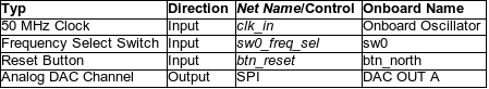
Table
1: Project Port Description
Note:
This design is based on the So-Logic Style Guide
1.3 Schematic
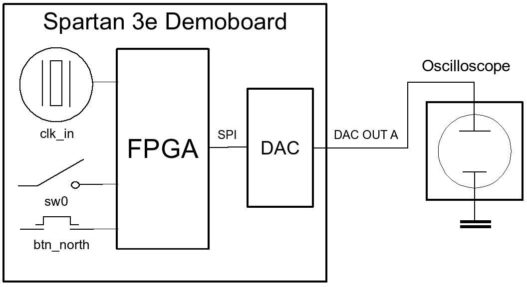
Drawing
1.3.1: Project Overview
1.4 Project Steps
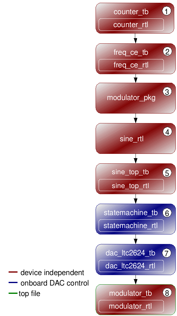
Drawing
1.4.1: Project Steps
Variable counter
module
Generate
two
triggered frequencies
(~1kHz
and ~3,5kHz)
dependent on the switch (sw0) state
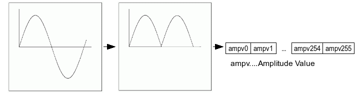
Generate
a quantized unsigned sine and store 255 amplitude values of
one sine-period into a ROM-Array
Device-independent
output of quantized unsigned sine from the modulator package
(modulator_pkg_rtl) with triggered frequency from the
freq_ce_rtl module.
Combine
counter_rtl, freq_ce_rtl, modulator_pkg_rtl and
sine_rtl module in top
file
Generate
a three
state
clocked Moore statemachine
with two outputs if state_en is set to high for SPI interface of dac
module
Fetch
the frequency and the amplitude values from the sine module
(sine_rtl) and generate the SPI signals for the
dac(ltc2624)
Connect all modules with
each other. Has got the interface for communicating with the
FPGA and the Onboard-DAC. Furthermore it disables other devices
on the spi-bus to avoid contention
1.5 Design Flow
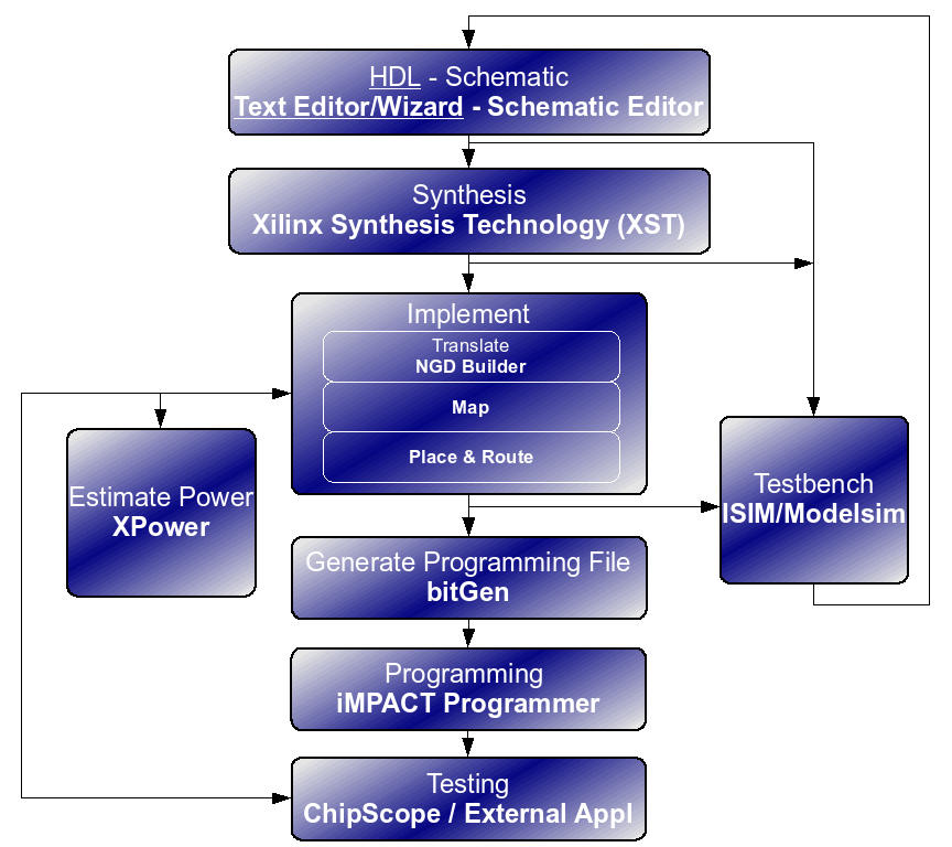
Drawing
1.5.1: Design Flow
Synthesize,
checks
code syntax and analyze the hierarchy of your design which ensures
that your design is optimized for the design architecture you have
selected. The resulting netlist is saved to an NGC file (for Xilinx®
Synthesis Technology (XST)) or an EDIF file
(for Precision, or Synplify/Synplify Pro)
Implement/Translate,
which merges the incoming netlists
and constraints into a binary database
Implement/Map,
which maps the design into the available resources on the target
device, like LUT, Flip Flops, BRAM,...
Implement/Place
and Route, which places and
routes the mapped database and checks the timing constraints
Generate
Programming File, which creates a bitstream file that can be
downloaded to the device
2. Modulator Counter
2.1 Description
Filename:
counter_rtl.vhd
Usage:
Generate an universal counter which divides an input clock, when the
counter is enabled, to a variable frequency dependent on the input
threshold generic value (half clock period)
Input:
clk_in:
input clock
cnt_en:
count enable
Output:
Schematic:
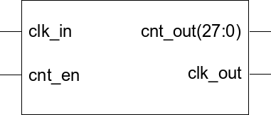
Drawing
2.1.1: Counter Schematic
Note:
This module is used as clock divider for an status led and as counter
(0 upto 256) for the dac_ltc2624_rtl module
2.2 Create Project
Launch Project Navigator
In the Project Navigator, select
File / New Project
Choose your Working Directory at
the Project Location field (*/)
Note: Automatically generates
projects folder, named from project name, in the working directory
Enter project_name
(modulator) in the
Project Name Field
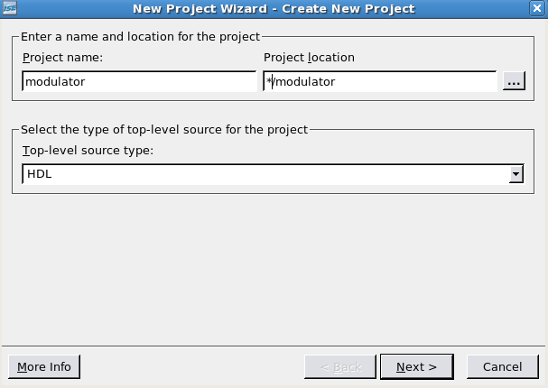
Illustration
2.1: Create New Project Dialog Box
Verify that HDL is
selected from the Top-Level Source Type drop-down list
Click Next
Set
the following parameters
Design
Purpose (like Automotive, Military / Hi-reliability,...)
Family
Specification (like Coolrunner, Spartan, Virtex,...)
Device
Type (like different number of CLBs, memory-, clock-resources,...
)
Different
package (type of package, size, number of IOs, type of IOs)
Leave
all other options at their default setting
Click
Next, leaving all fields blank in the Create New Source File
dialog box
Click
Next, leaving all fields blank in the Add Existing Sources
dialog box
Click
Finish in the Summary dialog box to create the new project
2.3 Create Module
Select Project / New
Source
In the New Source dialog box,
select VHDL Module, enter module_name (counter_rtl)
in the File name field an click Next to open the Define
Module dialog box
Enter module_entity_name
(counter)
in the Entity name field and module_architecture_typ (rtl)
in the Architecture name field
Enter the port data for the
intended module as shown in llustration: Define Module Dialog
Box
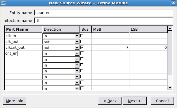
Illustration
2.2: Define Module Dialog Box
When you are finished, click
Next and click Finish
The Tool
automatically creates the entity declaration based an the data that
you entered and a default header.
Important:
The automatically generated code is not very handsome and clear, so
you should modify it:
--------------------------------------------------------------------------------
-- File        : counter_rtl.vhd
-- Project     : modulator
-- Creation    : 15.07.2008
-- Limitations : none
-- Errors      : none known
-- Simulator   : Modelsim SE 6.2a
-- Synthesizer : ISE 10.1
-- Platform    : Windows XP
-- Targets     : Simulation, Synthese
---------------------------------------
-- Naming conv. : so_vhdl_guide.doc
---------------------------------------
-- Authors      : Mario Fohler (mfo1)
-- Organization : so-logic
-- Email        : mfo1@so-logic.co.at
-- Address      : Lustkandlg. 52/22, A-1090 Vienna Austria/Europe/Earth
--------------------------------------------------------------------------------
-- Copyright Notice
-- Copying of this document and giving it to others and the
-- communication of the contents thereof is forbidden without authority.
-- Offenders are liable to payment of damages. All rights are reserved in
-- event of the grant or patent of the utility model or design.
--------------------------------------------------------------------------------
-- Function description
-- generate divided clock
--------------------------------------------------------------------------------
-- $HeadURL:$
-- $Date:$
-- $Author:$
-- $Revision:$
--------------------------------------------------------------------------------
set all text to lower case
remove
all end descriptions (for example: rtl
next to end) and all comments
set
all in/outputs in alphabetical order and comment them
library ieee;
    use ieee.std_logic_1164.all;
    use ieee.std_logic_arith.all;
    use ieee.std_logic_unsigned.all;

entity counter is
    port(
        clk_in  : in  std_logic; -- clk (50MHz)
        clk_out : out std_logic; -- divided clk
        cnt_out : out std_logic_vector(cnt_value_g'length - 1 downto 0); -- clk counter
        cnt_en  : in  std_logic  -- clk counter enable
    );
end;
Note:
As you can see there is much to modify. For better designs do not use
the GUI module inserter! Instead create an module in an text file
with an text editor, rename it to module_name.vhd
and insert it into your project (see chapter 3.2)
Now
add a variable (threshold value generic) and the variable
clock counter architecture after the entity.
counter_rtl
code:
library ieee;
    use ieee.std_logic_1164.all;
    use ieee.std_logic_arith.all;
    use ieee.std_logic_unsigned.all;

entity counter is
    generic(
        cnt_value_g : std_logic_vector -- threshold value for counter
    );

    port(
        clk_in  : in  std_logic; -- clk (50MHz)
        clk_out : out std_logic; -- divided clk
        cnt_out : out std_logic_vector(cnt_value_g'length - 1 downto 0); -- clk counter
        cnt_en  : in  std_logic  -- clk counter enable
    );
end;

architecture rtl of counter is

    signal clk_out_s    : std_logic := '0'; -- divided clk
    signal cnt_out_s : std_logic_vector (cnt_value_g'length - 1 downto 0) := (others => '0'); -- clk counter

begin

counter_p: process
begin

    wait until rising_edge(clk_in);
    if (cnt_en = '1') then
        clk_out_s <= cnt_out_s(cnt_value_g'length-2);
        if (cnt_out_s = cnt_value_g - 1) then
            cnt_out_s <= (others => '0'); -- counter reset
        else
            cnt_out_s <= cnt_out_s + 1;   -- counter
        end if;
    else
        clk_out_s <= '0';
    end if;

end process;

clk_out <= clk_out_s;
cnt_out <= cnt_out_s;

end;
In the Sources window, right-click on the module_name
(counter_rtl) , expand Synthesize and double-click
Check Syntax (see Illustration)
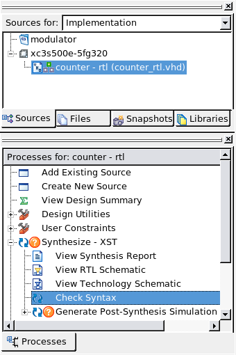
Illustration
2.3: Check Syntax
Correct any errors before proceeding
2.4 Create Test Bench
Create a test bench to simulate you
created clock counter.
Select Project / New
Source
In the New Source dialog box,
select VHDL Test Bench an
enter testbench_name
(counter_tb) in the
File name field.
Illustration
2.4: New Source Dialog Box
Click
Next
The next
dialog box prompts you for which module to associate with the
testbench file.
Select
the counter module. Click Next
and click Finish in
the Summary dialog box
The ISE
software now have created a standard structure for a test bench,
which contains:
Test
bench description
Component
declaration: Based on the Unit Under Test (UUT) that you designated
Signal
declarations: Using the same names as the ports on the UUT module
Time
constants for clock generation
Instantiation
and port map: Connected the declared component and signals
Clock
process definitions: Created three 1MHz outputs
Stimulus
process: Created wait statements for stimulus generation
Important:
The automatically generated code is not very handsome and clear, so
you should modify it:
set
all text to lower case
remove
all time constants, clock process definitions, stimulus process,
port map definition (uut: counter) and comments
rename
the architecture description to architecture tb of counter_tb
suffix all signals with a “_s” (for example: clk_in_s)
and update it in the port map on the right side
create
a module - (header) and a revision-description (footer) as comment
set
all in/outputs and signals in alphabetical order and comment them
Note:
As you can see there is much to modify. For better designs do not
use the GUI module inserter! Instead create an module in an text
file with an text editor, rename it to module_name.vhd and
insert into your project (see chapter 3.2)
Create
now an test bench with:
counter_tb
code:
library ieee;
    use ieee.std_logic_1164.all;
    use ieee.std_logic_arith.all;
    use ieee.std_logic_unsigned.all;

entity counter_tb is

    generic(
        clkcnt_value_g : std_logic_vector := b"100" -- threshold value for counter
    );

end;

architecture tb of counter_tb is

    constant per_c : time := 20 ns; -- clock period

    signal clk_in_s     : std_logic := '1'; -- clk (50MHz)
    signal clk_out_s    : std_logic := '0'; -- divided clk
    signal clkcnt_out_s : std_logic_vector (clkcnt_value_g'length - 1 downto 0) := (others => '0'); -- clk counter
    signal cnt_en_s     : std_logic := '1'; -- clk counter enable

begin

    counter : entity work.counter(rtl) -- fetch generic and ports of counter_rtl.vhd

        generic map(
            clkcnt_value_g => clkcnt_value_g
        )

        port map (
            clk_in     => clk_in_s,
            clk_out    => clk_out_s,
            clkcnt_out => clkcnt_out_s,
            cnt_en     => cnt_en_s
        );

    clk_in_s  <=  not (clk_in_s) after per_c/2; -- generate 50MHz clock
    cnt_en_s  <=  '0' after 300 ns; -- set clk counter enable to zero after 300ns
end;
2.5 Simulate (with ISIM)
After you have entered the code
for the input stimulus, select Source / Properties
Verify that ISE Simulator
(VHDL/Verilog) is selected in the Simulator field and VHDL
in the Preferred Language field (see Illustration 2.2.2)
Click Ok
Select testbench_name
(counter_tb.vhd) in
the Sources window
If necessary, select Behavioral
Simulation from the “Sources for” drop-down list
In the Processes window, expand
Xilinx ISE Simulator and double-click Check Syntax
(only available for ISE Simulator)
Illustration
2.5: Sources for and Processes Windows
Correct any errors before
proceeding.
In the processes window,
double-click Simulate Behavioral Model
Assuming
no errors, your simulation result should look similar to
Illustration
Illustration
2.6: Simulation Results
Optional:
If you want to insert further internal signals from your simulated
file, click on the file in the Sim Instances window and
drag-and-drop the signal from the Sim Objects window into the
waveform window. Now you have to restart and rerun your simulation
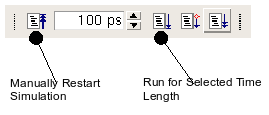
Optional:
Restart and rerun simulation for specific time
Illustration
2.7.: Variable Simulation Time
Note: In this design you can
choose about two different simulators, the integrated ISE Simulator
from Xilinx and Mentor's Modelsim-SE. How you can change to and use
the Modelsim Simulator switch to chapter 3.4
3. Modulator Frequency Triggger
3.1 Description
Filename:
freq_ce_rtl.vhd
Usage:
Generate two trigger frequencies (~1kHz
and ~3,5kHz)
dependent on the two-state input ('0' or '1')
Input:
Output:
Schematic:
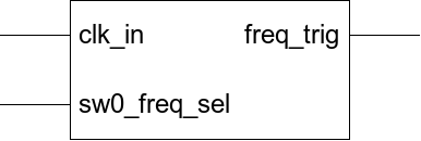
Drawing
3.1.1: Frequency Enable Schematic
3.2 Create Module
Note:
As you have seen before, there were much to modify for. For better
designs do not use the GUI module inserter!
Instead:
Open
any text editor (for better usability take one with vhdl
code support)
Insert
the vhdl code, add the counter_rtl module header and modify
it for this module
Save
the file as module_name (e.g. freq_ce_rtl) into your
working directory
Change
the ending from *.txt
to *vhd
Optional: Launch
Project Navigator (if not
open)
Optional: Open
Project Modulator (modulator.ise)
(if not open)
In
the Project Navigator, select Project
/ Add Source
Select
module file (e.g. freq_ce_rtl.vhd)
Select
All in the Design
View window
Click
Ok
freq_ce_rtl
code:
library ieee;
    use ieee.std_logic_1164.all;
    use ieee.std_logic_arith.all;
    use ieee.std_logic_unsigned.all;

entity freq_ce is
    generic(
        freqhigh_g : std_logic_vector (7 downto 0) := (others=>'0'); -- clk divider threshold for sw0_freq_sel = '1'
        freqlow_g  : std_logic_vector (7 downto 0) := (others=>'0')  -- clk divider threshold for sw0_freq_sel = '0'
    );
    port(
        clk_in       : in  std_logic; -- clk (50Mhz)
        freq_trig    : out std_logic; -- trigger period with selected frequency
        sw0_freq_sel : in  std_logic  -- select frequency
    );
end;

architecture rtl of freq_ce is

    signal freq_cnt_s       : std_logic_vector (7 downto 0) := (others => '0'); -- clock counter
    signal sw0_freq_sel_jmp : std_logic := '0'; -- change after sw0_freq_sel'event

begin

freq_ce_p : process -- create and select frequency

begin

    wait until rising_edge(clk_in);
    freq_cnt_s <= freq_cnt_s + 1; -- increment
    freq_trig <= '0';

    case sw0_freq_sel is -- select sine frequency

        when '0' => -- frequency for sw0_freq_sel = '0'
            if (sw0_freq_sel_jmp = '1') then
                freq_cnt_s <= (others => '0'); -- reset
                sw0_freq_sel_jmp <= '0';
            end if;
            if (freq_cnt_s = freqlow_g - 1) then
                freq_trig <= '1';
                freq_cnt_s <= (others => '0'); -- reset
            end if;

        when '1' => -- frequency for sw0_freq_sel = '1'
            if (sw0_freq_sel_jmp = '0') then
                freq_cnt_s <= (others => '0'); -- reset
                sw0_freq_sel_jmp <= '1';
            end if;
            if (freq_cnt_s = freqhigh_g - 1 ) then
                freq_trig <= '1';
                freq_cnt_s <= (others => '0'); -- reset
            end if;

        when others => null;

    end case;

end process;

end;
3.3 Create Test Bench
sw0_freq_sel: default “high”, after 500ns “low”
freqhigh_g:
set to b"1100_0011" (generate ~
25,6kHz frequency trigger)
freqlow_g:
set to b"1100_0011" (generate ~
909,1kHz frequency trigger)
Output:
Create
the frequency trigger testbench using the steps in chapter
3.2
with freq_ce_tb.vhd
file name and the following code
freq_ce_tb
code:
library ieee;
    use ieee.std_logic_1164.all;
    use ieee.std_logic_arith.all;
    use ieee.std_logic_unsigned.all;

entity freq_ce_tb is

    generic(
        freqhigh_g : std_logic_vector (7 downto 0) := b"0000_0100"; -- clk divider threshold sw0_freq_sel = '1'
        freqlow_g  : std_logic_vector (7 downto 0) := b"0000_0010"  -- clk divider threshold sw0_freq_sel = '0'
    );

end;

architecture tb of freq_ce_tb is

    constant per_c : time := 20 ns; -- clock period

    signal clk_in_s       : std_logic := '1';
    signal freq_trig_s    : std_logic := '1';
    signal sw0_freq_sel_s : std_logic := '0';

begin

    freq_ce : entity work.freq_ce(rtl) -- fetch generic and ports of fre_ce_rtl.vhd
        generic map(
            freqhigh_g => freqhigh_g,
            freqlow_g  => freqlow_g
        )
        port map(
            clk_in       => clk_in_s,      -- clk (50Mhz)
            freq_trig    => freq_trig_s,   -- trigger period with selected frequency
            sw0_freq_sel => sw0_freq_sel_s -- select frequency
        );

    clk_in_s       <=  not (clk_in_s) after per_c/2; -- generate 50MHz clock
    sw0_freq_sel_s <=  '1' after 200 ns;             -- set data to high after 200ns

end;
3.4 Simulate (with Modelsim)
After you have entered
the code for the input stimulus, select Source / Properties
Verify that Modelsim-SE VHDL
is selected in the Simulator field and VHDL in the Preferred
Language field and click Ok
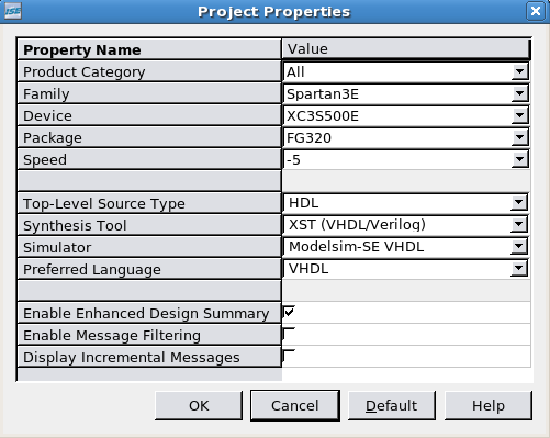
Illustration
3.1: Project Properties
Select testbench_name
(freq_ce_tb.vhd) in
the Sources window
If necessary, select Behavioral
Simulation from the “Sources for” drop-down list
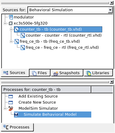
Illustration
3.2: Sources for and Processes Windows
In the Processes window, expand
ModelSim Simulator and double-click Simulate Behavioral
Model
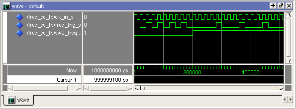
Illustration
3.3: Simulation Results
Assuming
no errors in the ModelSim command line, your simulation
result should look similar to Illustration
Optional:
If you want to insert further internal signals from your simulated
file, click on the file in the Sim Instances - workspace window and
drag-and-drop the signal from the Objects window into the waveform
window. Now you have to restart and rerun your simulation
Optional:
Restart and rerun simulation for specific time
Illustration
3.4.: Variable Simulation Time
Note:
In this design you can choose about two different simulators, the
integrated ISE Simulator from Xilinx and Mentor's Modelsim-SE. How
you can change to and use the ISE Simulator switch
to chapter 2.5
4. Modulator Package
4.1 Description
Drawing
4.1.1: Package Description
Note:
used in dac_ltc2624_rtl.vhd
4.2 Create Module
modulator_pkg
code:
library ieee;
    use ieee.math_real.all;
    use ieee.std_logic_1164.all;
    use ieee.std_logic_arith.all;
    use ieee.std_logic_unsigned.all;

package modulator_pkg is

    type vector_t_arr is array (natural range <>) of integer;

    function init_sin_f
        (
        constant depth_c : in integer;
        constant width_c : in integer
        )
    return vector_t_arr;

end;

package body modulator_pkg is

    function init_sin_f
        (
        depth_c : in integer;
        width_c : in integer
        )
    return vector_t_arr is

    variable init_arr_v : vector_t_arr(0 to (2 ** depth_c));

    begin

        for i in 0 to ((2 ** depth_c) / 2) loop -- calculate positive amplitude values
            init_arr_v(i) := integer(round(sin((math_2_pi / real(2 ** depth_c))*
                                     real(i)) * real(2 ** (width_c - 1)))) + integer(2 ** (width_c - 1) - 1);
        end loop;

        for i in ((2 ** depth_c) / 2 + 1) to (2 ** depth_c) loop -- calculate negativ amplitude values
            init_arr_v(i) := integer(round(sin((math_2_pi / real(2 ** depth_c))*
                                     real(i)) * real(2 ** (width_c - 1)))) - integer(2 ** (width_c - 1));
        end loop;

        return init_arr_v;

    end;

end;
5. Digital Sine
5.1 Description
Drawing
5.1.1: Sine RTL Schematic
5.2 Create Module
Create the sine_rtl using the steps
in chapter 3.2 with sine_rtl.vhd
file name and the following code
sine_rtl
code:
library ieee;
use ieee.std_logic_1164.all;
use ieee.std_logic_arith.all;
use ieee.std_logic_unsigned.all;
use work.modulator_pkg.all;
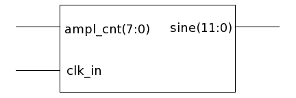
entity sine is
generic(
depth_g : integer range 1 to 99 := 8; -- sine signal 8bit quantized
width_g : integer range 1 to 99 := 12 -- 12 bit sine amplitude value
);
port(
ampl_cnt : in std_logic_vector(depth_g-1 downto 0); -- amplitude counter
sine : out std_logic_vector(width_g-1 downto 0); -- sine
clk_in : in std_logic -- 50MHz clock
);
end;
architecture rtl of sine is
constant sin_ampl_c : vector_t_arr := init_sin_f(depth_g, width_g); -- returns sine amplitude value
signal ampl_cnt_s : integer range 0 to 255 := 0; -- amplitude counter
signal sine_s : std_logic_vector(width_g-1 downto 0) := (others=>'0'); -- sine
begin
sine_p : process -- fetch amplitude values and frequency - generate sine
begin
wait until rising_edge(clk_in);
ampl_cnt_s <= conv_integer(ampl_cnt); -- convert amplitude counter into integer
sine_s <= conv_std_logic_vector(sin_ampl_c(ampl_cnt_s), width_g); -- fetch amplitude
end process;
sine <= sine_s;
end;
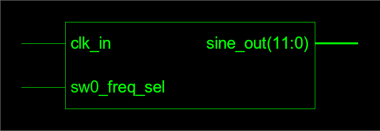
6. Digital Sine Top
6.1 Description
Filename:
sine_top_rtl.vhd
Usage: Connect the
sine_rtl module with the counterampl module (counter.vhd) with hex
“ff” threshold generic and the fre_ce module (freq_ce_rtl.vhd)
with the two selected frequencies
Input:
Output:
Schematic:
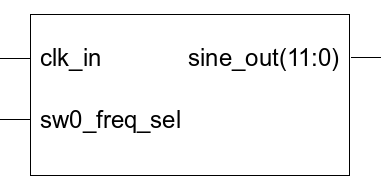
Drawing
6.1.1: Sine Top RTL Schematic
Drawing
6.1.2: Sine Top RTL Detailed Schematic
6.2 Create Module
Create the sine_rtl using the steps
in chapter 3.2 with sine_rtl.vhd
file name and the following code
sine_top_rtl
code:
library ieee;
    use ieee.std_logic_1164.all;
    use ieee.std_logic_arith.all;
    use ieee.std_logic_unsigned.all;

    use work.modulator_pkg.all;

entity sine_top is
    generic(
        cntampl_value_g : std_logic_vector := x"ff";
        depth_g         : integer range 1 to 99 := 8; -- sine signal 8bit quantized
        freqhigh_g      : std_logic_vector (7 downto 0) := b"1100_0011"; -- threshold value of frequency a
        freqlow_g       : std_logic_vector (7 downto 0) := b"0011_0111"; -- threshold value of frequency b
        width_g         : integer range 1 to 99 := 12 -- 12 bit sine amplitude value
    );
    port(
        clk_in       : in  std_logic; -- clk 50 MHz
        sine_out     : out  std_logic_vector(width_g-1 downto 0); -- sine
        sw0_freq_sel : in  std_logic -- frequency-select switch
    );
end;

architecture rtl of sine_top is

    constant sin_ampl_c : vector_t_arr := init_sin_f(depth_g, width_g); -- returns sine amplitude value

    signal ampl_cnt_s   : std_logic_vector(depth_g-1 downto 0) := (others=>'0'); -- amplitude counter
    signal freq_trig_s  : std_logic := '0';

begin

counterampl : entity work.counter(rtl) -- generate amplitude values
    generic map(
        cnt_value_g => cntampl_value_g -- clk counter threshold value
    )
    port map (
        clk_in  => clk_in,
        clk_out => open,
        cnt_out => ampl_cnt_s,
        cnt_en  => freq_trig_s
    );

freq_ce : entity work.freq_ce(rtl)
    generic map(
        freqhigh_g => freqhigh_g, -- clk divider threshold for sw0_freq_sel = '1'
        freqlow_g  => freqlow_g   -- clk divider threshold for sw0_freq_sel = '0'
    )
    port map(
        clk_in       => clk_in,      -- clk (50Mhz)
        freq_trig    => freq_trig_s, -- trigger period with selected frequency
        sw0_freq_sel => sw0_freq_sel -- select frequency
    );

sine : entity work.sine(rtl)
    generic map(
        depth_g => depth_g, -- sine signal 8bit quantized
        width_g => width_g  -- 12 bit sine amplitude value
    )
    port map(
        ampl_cnt => ampl_cnt_s, -- amplitude counter
        clk_in   => clk_in,      -- 50MHz clock
        sine     => sine_out   -- sine
    );

end;
6.3 Create Test Bench
Create
the frequency trigger testbench using the steps in chapter
3.2
with statemachine_tb.vhd
file name and the following code
library ieee;
    use ieee.std_logic_1164.all;
    use ieee.std_logic_arith.all;
    use ieee.std_logic_textio.all;
    use ieee.std_logic_unsigned.all;

entity sine_top_tb is
    generic(
        cntampl_value_g : std_logic_vector := x"ff";
        depth_g         : integer range 1 to 99 := 8; -- sine signal 8bit quantized
        freqhigh_g      : std_logic_vector (7 downto 0) := b"1100_0011"; -- threshold value of frequency a
        freqlow_g       : std_logic_vector (7 downto 0) := b"0011_0111"; -- threshold value of frequency b
        width_g         : integer range 1 to 99 := 12 -- 12 bit sine amplitude value
    );
end;

architecture tb of sine_top_tb is

    constant per_c : time := 20 ns; -- clock period

    signal clk_in_s       : std_logic := '0';
    signal sw0_freq_sel_s : std_logic := '0';
    signal sine_out_s     : std_logic_vector(width_g-1 downto 0) := (others=>'0');

begin

    dut : entity work.sine_top -- fetch generic and port of sine_top_rtl.vhd
        generic map(
            cntampl_value_g => cntampl_value_g,
            depth_g         => depth_g,
            freqhigh_g      => freqhigh_g,
            freqlow_g       => freqlow_g,
            width_g         => width_g
        )
        port map(
            clk_in       => clk_in_s,
            sw0_freq_sel => sw0_freq_sel_s,
            sine_out     => sine_out_s
        );

    clk_in_s  <=  not (clk_in_s) after per_c/2; -- generate 50MHz clock
    sw0_freq_sel_s <= '0', '1' after 1 ms;      -- sw0_freq_sel high, low after variable time

end;
6.4 Simulate
Choose your simulator:
Simulate 10 μs
Display
digital as analog sine (Only available for ModelSim!)
Zoom
In/Out to see all simulated signals
Right-click
on sine_out_s
Select
Format / Analog
Illustration
6.1: Display analog sine
Format:
Analog Step
Click
Ok
Right-click
on sine_out_s again
Select
Radix / Unsigned
Assuming no errors,
your simulation result should look similar to Illustration
Illustration
6.2: Sine Simulation
6.5 Synthesize
6.5.1 Description
Synthesize,
checks code
syntax
and analyze
the hierarchy
of your design
which ensures that your design is optimized for the design
architecture you have selected (e.g. Number of flip flops, LUTs,
Clock- and IO-Buffers) The resulting netlist is saved to an NGC file
(for Xilinx® Synthesis Technology (XST)) or an EDIF file (for
Precision, or Synplify/Synplify Pro).
ISE Synthesize Utility: XST
(Xilinx Synthesize Technology)
6.5.2 Synthesize
In the Sources window,
right-click on the synthesizeable module (sine_top_rtl)
and select Set as Top Module (see
Illustration), if
not set
Illustration
6.3: Set as Top Module
In the Sources window, select
synthesizeable module (sine_top_rtl). In Process
window, double-click Synthesize – XST (see
Illustration)
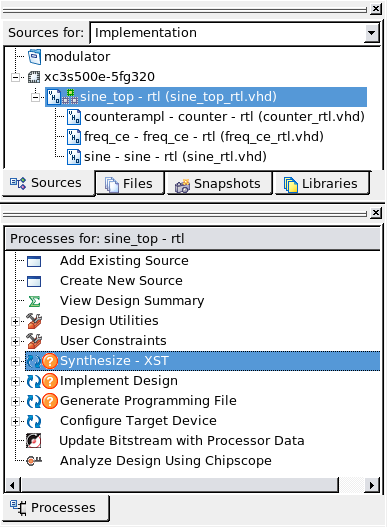
Illustration
6.4: Synthesize
6.5.3 Synthesis Report
Shows IO and logic devices use
=========================================================================
*                            Final Report                               *
=========================================================================
Final Results
RTL Top Level Output File Name     : freq_ce.ngr
Top Level Output File Name         : freq_ce
Output Format                      : NGC
Optimization Goal                  : Speed
Keep Hierarchy                     : NO

Design Statistics
# IOs                              : 3

Cell Usage :
# BELS                             : 30
#      GND                         : 1
#      INV                         : 1
#      LUT1                        : 7
#      LUT2                        : 2
#      LUT4                        : 1
#      LUT4_D                      : 2
#      MUXCY                       : 7
#      VCC                         : 1
#      XORCY                       : 8
# FlipFlops/Latches                : 10
#      FDE                         : 1
#      FDR                         : 9
# Clock Buffers                    : 1
#      BUFGP                       : 1
# IO Buffers                       : 2
#      IBUF                        : 1
#      OBUF                        : 1
=========================================================================
=========================================================================
HDL Synthesis Report

Macro Statistics
# Counters                                             : 1
 8-bit up counter                                      : 1
# Registers                                            : 2
 1-bit register                                        : 2

=========================================================================
Device utilization summary:
---------------------------

Selected Device : 3s500efg320-5

 Number of Slices:                        8  out of   4656     0%
 Number of Slice Flip Flops:             10  out of   9312     0%
 Number of 4 input LUTs:                 13  out of   9312     0%
 Number of IOs:                           3
 Number of bonded IOBs:                   3  out of    232     1%
 Number of GCLKs:                         1  out of     24     4%
6.5.4 RTL Schematic
Create an logic circuit of your
designed module
In the Sources window,
right-click on the synthesizeable module (sine_top_rtl)
, expand Synthesize and double-click View RTL Schematic
Illustration
6.5: View RTL Schematic
Optional:
If you want a detailed view of your design, double-click
on the schematic to zoom-in

Illustration
6.6: View RTL Schematic detailed
6.5.5 Technology Schematic
Shows logical schematic like an RTL
Schematic, but without module blackboxes (levels)
6.5.6 Check Syntax
6.5.7 Generate Post-Synthesis Simulation Model
You can generate a simulation model
after synthesizing your design. For this process, NetGen converts the
synthesis output (NGC) to a simulation model (a structural
UNISIM-based VHDL or Verilog file). The simulation model can be used
to verify that the functionality is correct after synthesis by
running a post-synthesis simulation in your simulator.
In the Processes window,
expand Synthesize – XST
Right-click
on Generate Post-Synthesis Simulation Model / Properties,
Rename Top-Level Architecture To rtl, click Ok
Note:
Verify that the Advanced Property Display Level is enabled
Double-click Generate
Post-Synthesis Simulation Model
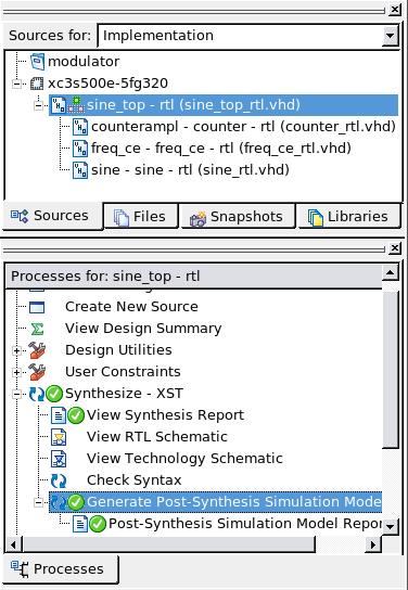
Illustration
6.7: Generate Post-Synthesis Simulation Model
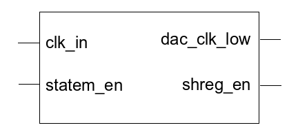
7. Modulator Finite Statemachine
7.1 Description
Filename: state
machine_rtl.vhd
Usage:
Generate a clocked Moore state machine with three states (shreg_end,
shreg_start, clk_pause) and two output signals (shreg_en,
dac_clk_low) for the interface of the dac module. The state machine
will start, if the state machine enable (statem_en) is set to high.
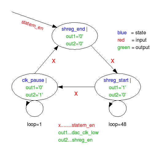
Drawing
7.1.1: Statemachine
Drawing
7.1.2: Statemachine Schematic
7.2 Create Module
statemachine_rtl
code:
library ieee;
    use ieee.std_logic_1164.all;
    use ieee.std_logic_arith.all;
    use ieee.std_logic_unsigned.all;

entity statemachine is
    port(
        clk_in      : in  std_logic; -- 50MHz clock
        dac_clk_low : out std_logic; -- set dac clk to zero
        shreg_en    : out std_logic; -- shiftregister enable
        statem_en   : in  std_logic  -- statemachine enable
    );
end;

architecture rtl of statemachine is

    type state_type_t_enum is (shreg_end,shreg_start,clk_pause); -- three states of state machine

    signal dac_clk_low_s : std_logic := '0';  -- set dac clk low
    signal shreg_en_s    : std_logic := '0';  -- set shiftreg enable low
    signal statem_loop_s : integer range 0 to 49 := 0; -- state loop
    signal statem_s      : state_type_t_enum; -- enumerated state machine

begin

statem_statereg_p : process -- shift states

begin

    wait until rising_edge(clk_in);
    if ((statem_en = '1') or  (dac_clk_low_s = '1')) then

        case statem_s is

            when shreg_end =>
                    statem_s <= shreg_start;

            when shreg_start =>
                if (statem_loop_s = 48) then
                    statem_s <= clk_pause;
                    statem_loop_s <= 0;
                else
                    statem_loop_s <= statem_loop_s + 1;
                end if;

            when clk_pause =>
                if (statem_loop_s = 1) then
                    statem_s <= shreg_end;
                    statem_loop_s <= 0;
                else
                    statem_loop_s <= statem_loop_s + 1;
                end if;

            when others => null;

        end case;

    end if;

end process;

statem_stateoutput_p : process(statem_s) -- define output to state

begin

    case statem_s is -- generate shiftregister enable and clk output low signal

        when shreg_start =>
            shreg_en_s <= '1';    -- start shift register
            dac_clk_low_s <= '0';

        when clk_pause =>
            shreg_en_s <= '0';    -- end shift register
            dac_clk_low_s <= '1'; -- set dac clk low

        when shreg_end =>
            shreg_en_s <= '0';
            dac_clk_low_s <= '0';

        when others => null;

    end case;

end process;

shreg_en    <= shreg_en_s;
dac_clk_low <= dac_clk_low_s;

end;
7.3 Create Test Bench
Create
the frequency trigger testbench using the steps in chapter
3.2
with statemachine_tb.vhd
file name and the following code
statemachine_tb
code:
library ieee;
    use ieee.std_logic_1164.all;
    use ieee.std_logic_arith.all;
    use ieee.std_logic_unsigned.all;

entity statemachine_tb is
end;

architecture tb of statemachine_tb is

    constant per_c : time := 20 ns; -- clock period

    signal clk_in_s      : std_logic := '1';
    signal dac_clk_low_s : std_logic := '0';
    signal shreg_en_s    : std_logic := '0';
    signal statem_en_s   : std_logic := '0';

begin

statemachine: entity work.statemachine(rtl)
    port map(
        clk_in      => clk_in_s,
        dac_clk_low => dac_clk_low_s,
        shreg_en    => shreg_en_s,
        statem_en   => statem_en_s
    );

clk_in_s  <=  not (clk_in_s) after per_c/2; -- generate 50MHz clock
statem_en_s <= '1' after 500 ns;

end;
7.4 Simulate
Choose your simulator:
Simulate 4 μs
Assuming no errors, your
simulation result should look similar to Illustration
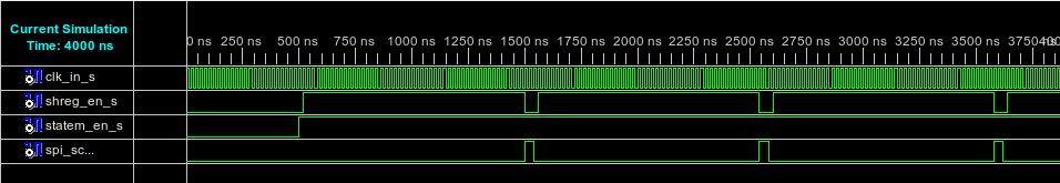
Illustration
7.1: Simulate Testbench
7.5 Implement/Translate
7.5.1 Description
Translate,
merges all of the input netlists and design constraints and outputs
a Xilinx native generic database (NGD) file, which describes the
logical design reduced to Xilinx primitives.
ISE Translate Utility: NGD
Builder
7.5.2 Generate UCF File
For this module no ucf file is
necessary, because it will not separately be integrated on the
device.
Note: Default the NGD Builder
generates an empty ucf-file, which means that there are no specific
port and timing constraints necessary, during the translating
process.
7.5.3 Translate
In the Sources window,
right-click on the translateable module (statemachine_rtl)
and select Set as Top Module,
if not set
In
the Sources window, select translateable module
(statemachine_rtl). In Process window, expand Implementation
Design and double-click Translate
(see Illustration )
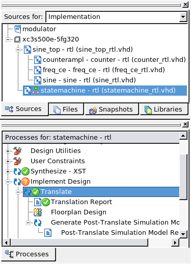
Illustration
7.2: Translate Statemachine
7.5.4 Translation Report
Displays NGDBUILD Design Results
Summary
7.5.5 Floorplan Design
Floorplanner™ interactive graphical
tool to perform the following functions on your designs:
Doing detailed-level
floorplanning
Creating an Relationally Placed
Macro (RPM) core that can be used in other designs
Viewing and editing location
constraints
Finding logic or nets by name or
connectivity
Cross probing from the Timing
Analyzer to the Floorplanner
Placing ports automatically for
modular design (part of a design
The
graphical user interface includes pull-down menus and toolbar buttons
that contain the necessary commands for changing the design
hierarchy, floorplanning, and performing design rule checks. Dialog
boxes allow you to set parameters and options for command execution.
Note: For more information and
instructions please read in the Floorplanner Help
7.5.6 Generate Post-Translate Simulation Model
NetGen converts the Translate
process output (an NGD file) to a post-translate simulation model (a
structural SIMPRIM-based VHDL and Verilog file).
Used in the Simulate
Post-Translate Model process to verify that design functionality is
correct after the translation stage or/and input file for your
simulator.
In the Processes
window, expand Implement / Translate
Right-click
on Generate Post-Translate Simulation Model / Properties,
Rename Top-Level Architecture To rtl, click Ok
Note:
Verify that the Advanced Property Display Level is enabled
Double-click
Generate Post-Synthesis Simulation Model
7.5.7 Performing Post-Translate Simulation
In
the
Sources
tab,
select Post-Translate
Simulation
from the drop-down list.
Select
a test bench file (statemachine_tb),
double-click on Simulation
Post-Translate Model
to run the simulation
The
generated waveform should fit with the graphic in the behaviour
simulation (see Illustration
6.1: Simulate Testbench)
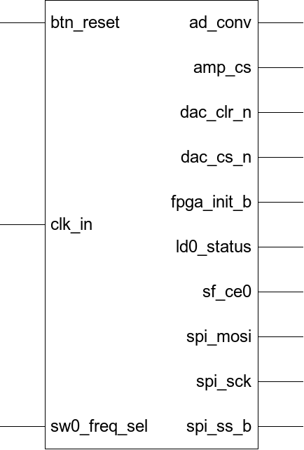
8. Modulator DAC
8.1 Description
Filename:
dac_ltc2624_rtl.vhd
Usage: Fetch the
frequency and the amplitude values from the frequented sine
amplitude signal (sine) and generates the SPI control signals
(dac_clk, dac_cs_n, dac_data, dac_reset_n) for the dac(ltc2624)
Input:
btn_reset: reset button
clk_in: clock
clkdv_in: divided clock by two
freq_trig: frequency of dac
data packages
sine: frequented sine amplitude
Output:
Schematic:
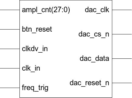
Drawing
8.1.1: DAC Schematic
Note: For
detailed description about the DAC please look in the DAC datasheet
in your working directory (*/modulator/docs/datasheet/2604fb.pdf)
8.2 Create Module
library ieee;
    use ieee.std_logic_1164.all;
    use ieee.std_logic_arith.all;
    use ieee.std_logic_unsigned.all;

    use work.modulator_pkg.all;

entity dac_ltc2624 is
    generic(
        depth_g : integer range 1 to 99 := 8;
        width_g : integer range 1 to 99 := 12
    );
    port(
        btn_reset   : in  std_logic; -- reset button
        clk_in      : in  std_logic; -- 50MHz clock
        clkdv_in    : in  std_logic; -- 25MHz clock
        dac_clk     : out std_logic; -- dac clock
        dac_cs_n    : out std_logic; -- dac enable
        dac_data    : out std_logic; -- dac data
        dac_reset_n : out std_logic; -- dac reset
        freq_trig   : in  std_logic; -- frequency of dac data packages
        sine        : in  std_logic_vector(width_g-1 downto 0) -- frequented sine amplitude
    );
end;

architecture rtl of dac_ltc2624 is

    signal dac_amplvalue_s    : std_logic_vector (sine'length-1 downto 0) := (others => '0'); -- 12 bit sine amplidude value
    signal dac_clk_low_s      : std_logic := '0';  -- set dac clk low
    signal dac_clk_s          : std_logic := '1';  -- dac clk signal
    signal dac_cs_n_s         : std_logic := '1';  -- dac enable signal
    signal dac_out_serial_s   : std_logic := '1';  -- dac output signal serial
    signal shreg_en_s         : std_logic := '0';  -- shift register enable
    signal shreg_s            : std_logic_vector (23 downto 0) := x"300000"; -- parallel2serial shift register
    signal shreg_update_s     : std_logic := '0';  -- update shiftregister with actual amplitude value
    signal statem_en_clkcnt_s : integer range 0 to 100 := 0; -- clock counter of state machine enable
    signal statem_en_s        : std_logic := '0';  -- state machine enable

begin

statemachine : entity work.statemachine(rtl)-- generate statemachine for shiftregister enable and setting spi sck to low
    port map(
        clk_in => clk_in,
        dac_clk_low => dac_clk_low_s,
        statem_en => statem_en_s,
        shreg_en => shreg_en_s
    );

dac_signaloutput_p : process -- fetch amplitude values and generate dac output signals

begin

    wait until rising_edge(clk_in);
---- generate dac reset ------------------------------------------------------------------------------------------------
    if (btn_reset = '1') then
        dac_reset_n <= '0'; -- dac reset (active low)
    else
        dac_reset_n <= '1'; -- dac reset (active low)
    end if;
------------------------------------------------------------------------------------------------------------------------
---- activate statemachine and update shift register -------------------------------------------------------------------
    if (freq_trig = '1') then
        statem_en_s <= '1'; -- activate statemachine
        shreg_update_s <= '1';
    end if;
------------------------------------------------------------------------------------------------------------------------
---- deactivate statemachine -------------------------------------------------------------------------------------------
    if (statem_en_s = '1') then
        if (statem_en_clkcnt_s = 51) then
            statem_en_s <= '0';      -- deactivate statemachine
            statem_en_clkcnt_s <= 0; -- reset counter
        else
            statem_en_clkcnt_s <= statem_en_clkcnt_s+1;
        end if;
    end if;
------------------------------------------------------------------------------------------------------------------------
    dac_cs_n_s <= not shreg_en_s; -- generate dac enable
    dac_amplvalue_s <= sine;
---- update shift register ---------------------------------------------------------------------------------------------
    if (shreg_update_s = '1') and (shreg_en_s = '1') then
        shreg_s <= x"300000";                    -- load dac header (command and address code)
        shreg_s(15 downto 4) <= dac_amplvalue_s; -- load amplitude value into shift register
        shreg_update_s <= '0';
    end if;
------------------------------------------------------------------------------------------------------------------------
---- set default values ------------------------------------------------------------------------------------------------
    dac_out_serial_s <= '1';
    dac_clk_s <= '1';
------------------------------------------------------------------------------------------------------------------------
---- generate spi_sck and spi_mosi -------------------------------------------------------------------------------------
    if (shreg_en_s = '1') or (dac_clk_low_s = '1') then
        if (dac_clk_low_s = '0') then -- generate dac clk
            dac_clk_s <= not clkdv_in;
            if (dac_clk_s = '0') then
                shreg_s <= shreg_s (22 downto 0) & '0'; -- shift left and insert lsb '0'
            end if;
        else
            dac_clk_s <= '0';
        end if;
        dac_out_serial_s <= shreg_s(23); -- shiftregister output (parallel2serial)
    end if;
------------------------------------------------------------------------------------------------------------------------
end process;

    dac_cs_n <= dac_cs_n_s;       -- dac enable
    dac_clk  <= dac_clk_s;        -- dac clock
    dac_data <= dac_out_serial_s; -- dac output

end;
8.3 Implement/Map
8.3.1 Description
The
Map process maps the logic defined by an NGD file into FPGA elements,
such as CLBs and IOBs. The output design is a native circuit
description (NCD) file that physically represents the design mapped
to the components in the Xilinx FPGA.
8.3.2 Mapping
In the Sources window,
right-click on the mapping module (dac_ltc2624_rtl)
and select Set as Top Module,
if not set
In
the Sources window, select mapping module (dac_ltc2624_rtl).
In Process window, expand Implementation Design and
double-click Map (see
Illustration )
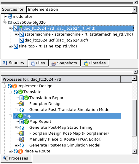
Illustration
8.1: Mapping DAC
8.3.3 Map Report
Design Summary
--------------
Number of errors:      0
Number of warnings:    0
Logic Utilization:
  Number of Slice Flip Flops:            38 out of   9,312    1%
  Number of 4 input LUTs:                56 out of   9,312    1%
Logic Distribution:
  Number of occupied Slices:             30 out of   4,656    1%
    Number of Slices containing only related logic:      30 out of      30 100%
    Number of Slices containing unrelated logic:          0 out of      30   0%
      *See NOTES below for an explanation of the effects of unrelated logic.
  Total Number of 4 input LUTs:          56 out of   9,312    1%
  Number of bonded IOBs:                 20 out of     232    8%
    IOB Flip Flops:                      15
  Number of BUFGMUXs:                     1 out of      24    4%

Peak Memory Usage:  161 MB
Total REAL time to MAP completion:  9 secs
Total CPU time to MAP completion:   3 secs
Section 13 - Control Set Information
Section 14 - Utilization by Hierarchy

Section 1 - Errors
------------------

Section 2 - Warnings
--------------------

Section 3 - Informational
-------------------------
INFO:MapLib:562 - No environment variables are currently set.
INFO:LIT:244 - All of the single ended outputs in this design are using slew
   rate limited output drivers. The delay on speed critical single ended outputs
   can be dramatically reduced by designating them as fast outputs.

Section 4 - Removed Logic Summary
---------------------------------
   1 block(s) optimized away

Section 5 - Removed Logic
-------------------------

Optimized Block(s):
TYPE 		BLOCK
VCC 		XST_VCC

To enable printing of redundant blocks removed and signals merged, set the
detailed map report option and rerun map.

Section 6 - IOB Properties
--------------------------

+----------------------------------------------------------------------------------------------------------------------------------------+
| IOB Name                           | Type             | Direction | IO Standard | Drive    | Slew | Reg (s)      | Resistor | IOB      |
|                                    |                  |           |             | Strength | Rate |              |          | Delay    |
+----------------------------------------------------------------------------------------------------------------------------------------+
| btn_reset                          | IBUF             | INPUT     | LVCMOS25    |          |      |              |          | 0 / 0    |
| clk_in                             | IBUF             | INPUT     | LVCMOS25    |          |      |              |          | 0 / 0    |
| clkdv_in                           | IBUF             | INPUT     | LVCMOS25    |          |      |              |          | 0 / 0    |
| dac_clk                            | IOB              | OUTPUT    | LVCMOS25    | 12       | SLOW |              |          | 0 / 0    |
| dac_cs_n                           | IOB              | OUTPUT    | LVCMOS25    | 12       | SLOW | OFF1         |          | 0 / 0    |
| dac_data                           | IOB              | OUTPUT    | LVCMOS25    | 12       | SLOW | OFF1         |          | 0 / 0    |
| dac_reset_n                        | IOB              | OUTPUT    | LVCMOS25    | 12       | SLOW | OFF1         |          | 0 / 0    |
| freq_trig                          | IBUF             | INPUT     | LVCMOS25    |          |      |              |          | 0 / 0    |
| sine<0>                            | IBUF             | INPUT     | LVCMOS25    |          |      | IFF1         |          | 0 / 3    |
| sine<1>                            | IBUF             | INPUT     | LVCMOS25    |          |      | IFF1         |          | 0 / 3    |
| sine<2>                            | IBUF             | INPUT     | LVCMOS25    |          |      | IFF1         |          | 0 / 3    |
| sine<3>                            | IBUF             | INPUT     | LVCMOS25    |          |      | IFF1         |          | 0 / 3    |
| sine<4>                            | IBUF             | INPUT     | LVCMOS25    |          |      | IFF1         |          | 0 / 3    |
| sine<5>                            | IBUF             | INPUT     | LVCMOS25    |          |      | IFF1         |          | 0 / 3    |
| sine<6>                            | IBUF             | INPUT     | LVCMOS25    |          |      | IFF1         |          | 0 / 3    |
| sine<7>                            | IBUF             | INPUT     | LVCMOS25    |          |      | IFF1         |          | 0 / 3    |
| sine<8>                            | IBUF             | INPUT     | LVCMOS25    |          |      | IFF1         |          | 0 / 3    |
| sine<9>                            | IBUF             | INPUT     | LVCMOS25    |          |      | IFF1         |          | 0 / 3    |
| sine<10>                           | IBUF             | INPUT     | LVCMOS25    |          |      | IFF1         |          | 0 / 3    |
| sine<11>                           | IBUF             | INPUT     | LVCMOS25    |          |      | IFF1         |          | 0 / 3    |
+----------------------------------------------------------------------------------------------------------------------------------------+

Section 7 - RPMs
----------------

Section 8 - Guide Report
------------------------
Guide not run on this design.

Section 9 - Area Group and Partition Summary
--------------------------------------------

Partition Implementation Status
-------------------------------

  No Partitions were found in this design.

-------------------------------

Area Group Information
----------------------

  No area groups were found in this design.

----------------------

Section 10 - Modular Design Summary
-----------------------------------
Modular Design not used for this design.

Section 11 - Timing Report
--------------------------
This design was not run using timing mode.

Section 12 - Configuration String Details
-----------------------------------------
Use the "-detail" map option to print out Configuration Strings

Section 13 - Control Set Information
------------------------------------
No control set information for this architecture.

Section 14 - Utilization by Hierarchy
-------------------------------------
+-------------------------------------------------------------------------------------------------------------------------------------------------------------------+
| Module             | Partition | Slices        | Slice Reg     | LUTs          | LUTRAM        | BRAM      | MULT18X18 | BUFG  | DCM   | Full Hierarchical Name   |
+-------------------------------------------------------------------------------------------------------------------------------------------------------------------+
| dac_ltc2624/       |           | 22/33         | 30/38         | 37/56         | 0/0           | 0/0       | 0/0       | 1/1   | 0/0   | dac_ltc2624              |
| +statemachine      |           | 11/11         | 8/8           | 19/19         | 0/0           | 0/0       | 0/0       | 0/0   | 0/0   | dac_ltc2624/statemachine |
+-------------------------------------------------------------------------------------------------------------------------------------------------------------------+

* Slices can be packed with basic elements from multiple hierarchies.
  Therefore, a slice will be counted in every hierarchical module
  that each of its packed basic elements belong to.
** For each column, there are two numbers reported <A>/<B>.
   <A> is the number of elements that belong to that specific hierarchical module.
   <B> is the total number of elements from that hierarchical module and any lower level
   hierarchical modules below.
*** The LUTRAM column counts all LUTs used as memory including RAM, ROM, and shift registers.
8.3.4 Post-Map Static Timing
The Timing Analyzer performs a
static timing analysis on the FPGA designs after mapping
Timing Analyzer:
reports
path delay and the slack based upon the specified
timing requirements.
analyze critical paths in
a circuit,
the cycle time of the
circuit,
quick analysis of the effect
speed grades, voltage, and temperature
prorating have on the same design
set up and hold checks
(works with synchronous systems comprising synchronous elements and
combinatorial logic)
creates timing analysis
reports based on timing constraints or user-specified paths
within the program.
uses
Timing
Wizard
for all FPGA analysis functions, ensuring consistency with PAR
Note: For more information and
instructions please read in the Timing Analyzer Help
8.3.5 Floorplan Design Post-Map
Floorplanner (see 6.5.5)
8.3.6 Manually Place & Route
FPGA Editor:
display and configure
FPGAs
requires a Native Circuit
Description (.ncd) file (logic of your design mapped to
components - such as CLBs and IOBs)
reads from and writes to a
Physical Constraints File (PCF).
The following is a list of a few of
the functions you can perform on your designs in the FPGA Editor.
Place and route critical
components before running the automatic place and route tools.
Finish placement and routing
if the routing program does not completely route your design.
Add probes to your design
to examine the signal states of the targeted device. Probes are used
to route the value of internal nets to an IOB for analysis during
the debugging of a device.
Cross-probe your design
with Timing Analyzer.
Run
the BitGen program and download the resulting BIT file
to the targeted device.
View
and change the nets
connected to the capture units of an ILA core in your design.
Create
an entire design by hand (advanced users).
8.3.7 Generate Post-Map Simulation Model
In the Sources window,
right-click on the simulating module (statemachine_tb)
In the Processes
window, expand Implement / Map
Right-click
on Generate Post-Translate Simulation Model / Properties,
Rename Top-Level Architecture To rtl, click Ok
Note:
Verify that the Advanced Property Display Level is enabled
Double-click
Generate Post-Synthesis Simulation Model
8.3.8 Performing Post-Map Simulation
In
the
Sources
tab,
select Post-Map
Simulation
from the drop-down list.
Select
a test bench file (statemachine_tb),
double-click on Simulation
Post-Translate Model
to run the simulation
The
generated waveform should fit with the graphic in the behaviour
simulation (see Illustration
6.1: Simulate Testbench)
8.4 Implement/Place&Route
8.4.1 Description
The
Place and Route process takes a mapped NCD file, places and routes
the design, and produces an NCD file that is used as input for
bitstream generation.
8.4.2 Place & Route
In the Sources window,
right-click on the place&route module (dac_ltc2624_rtl)
and select Set as Top Module,
if not set
In
the Sources window, select mapping module (dac_ltc2624_rtl).
In Process window, expand Implementation Design and
double-click Map (see
Illustration )
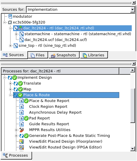
Illustration
8.2: Place&Route DAC
8.4.3 Place & Route Report
Design Summary Report:

 Number of External IOBs                          20 out of 232     8%

   Number of External Input IOBs                 16

      Number of External Input IBUFs             16

   Number of External Output IOBs                 4

      Number of External Output IOBs              4

   Number of External Bidir IOBs                  0


   Number of BUFGMUXs                        1 out of 24      4%
   Number of Slices                         30 out of 4656    1%
      Number of SLICEMs                      0 out of 2328    0%


Overall effort level (-ol):   Standard
Placer effort level (-pl):    High
Placer cost table entry (-t): 1
Router effort level (-rl):    Standard
8.4.4 Post-Place & Route Static Timing
The Timing Analyzer performs a
static timing analysis on the FPGA designs after place&route
(see 7.3.4)
8.4.5 View/Edit Placed Design (Floorplanner)
Floorplanner (see 6.5.5)
8.4.6 View/Edit Routed Design (FPGA Editor)
FPGA Editor (see 7.3.6)
8.4.7 XPower Analyzer
Analyze Power consumption
for Xilinx® FPGA and CPLD devices
Report thermal information
(junction temperature)
Report power information
Validate the accuracy
of the estimation given in Xilinx Power Estimator
Hierarchical power reporting
Examination
for power
reduction
8.4.8 Generate Post-Place & Route
Simulation Model
Analyze
the timing results of the Post-Place and Route process.
Reports
incorporate all delays to provide a comprehensive timing
summary.
Fixing
timing problems by increasing
the placer
effort level,
by using re-entrant routing, or by using multi-pass place and route.
Redesign
the logic
paths
to use fewer levels of logic, to tag the paths for specialized
routing resources, to move to a faster device, or to allocate more
time for the paths.
In the Sources window,
right-click on the simulating module (statemachine_tb)
In the Processes
window, expand Implement / Place & Route
Right-click
on Generate Post-Translate Simulation Model / Properties,
Rename Top-Level Architecture To rtl, click Ok
Note:
Verify that the Advanced Property Display Level is enabled
Double-click Generate
Post-Synthesis Simulation Model
8.4.9 Performing Post-Map Simulation
In
the
Sources
tab,
select Post-Route
Simulation
from the drop-down list.
Select
a test bench file (statemachine_tb),
double-click on Simulation
Post-Place Model
to run the simulation
The
generated waveform should fit with the graphic in the behaviour
simulation (see Illustration
6.1: Simulate Testbench)
8.4.10 Generate IBIS Model
IBIS
is a device modelling standard that allows for the development of
behavioral models used to describe the signal behavior
of device I/Os, while preserving proprietary circuit
information.
Best
and worst case models by using min, max current with the
proper min, max ramp rates.
Simulate
and predict electrical performance by providing I/V and V/T
characteristics of the I/Os.
Input
source:
8.4.11 Back-annotate Pin Locations
Runs
the PIN2UCF program which back-annotates pin-locking constraints
from a successfully placed and routed FPGA design to a user
constraints file (UCF).
Extracts
pin locations and logical pad names from the NCD file and writes
this information to an existing UCF. If a UCF does not exist
in your project, a new file is created.
Note:
By
default, PIN2UCF does not write conflicting constraints to a UCF. If
user-specified constraints are exact matches of PIN2UCF generated
constraints, a pound sign (#) is added in front of all matching
user-specified location constraint statements. If PIN2UCF discovers
conflicting constraints, it writes this information to the
pinlock.rpt report file.
9. Modulator Top
9.1 Description
Filename:
modulator_rtl.vhd
Usage: This Module
connects the modules with each other and has got the interface which
communicates with the FPGA (btn_reset, clk_in, sw0_freq_sel) and the
Onboard-DAC (dac_clr_n, dac_cs_n, spi_sck, spi_mosi). Furthermore it
disables other devices on the spi-bus to avoid contention (ad_conv,
amp_cs, fpga_init_b, sf_ce0, spi_ss_b)
Input:
Output:
ad_conv:
default '0' set for error-free dac use
amp_cs:
default '1' set for error-free dac use
dac_clr_n:
dac reset (active low)
dac_cs_n:
dac enable (active low)
fpga_init_b:
default '1' set for error-free dac use
ld0_status:
led clk (~0.5 Hz)
sf_ce0:
default '1' set for error-free dac use
spi_sck:
dac clk
spi_mosi:
dac output data
spi_ss_b:
default '1' set for error-free dac use
Schematic:
Drawing
9.1.1: Modulator RTL Schematic
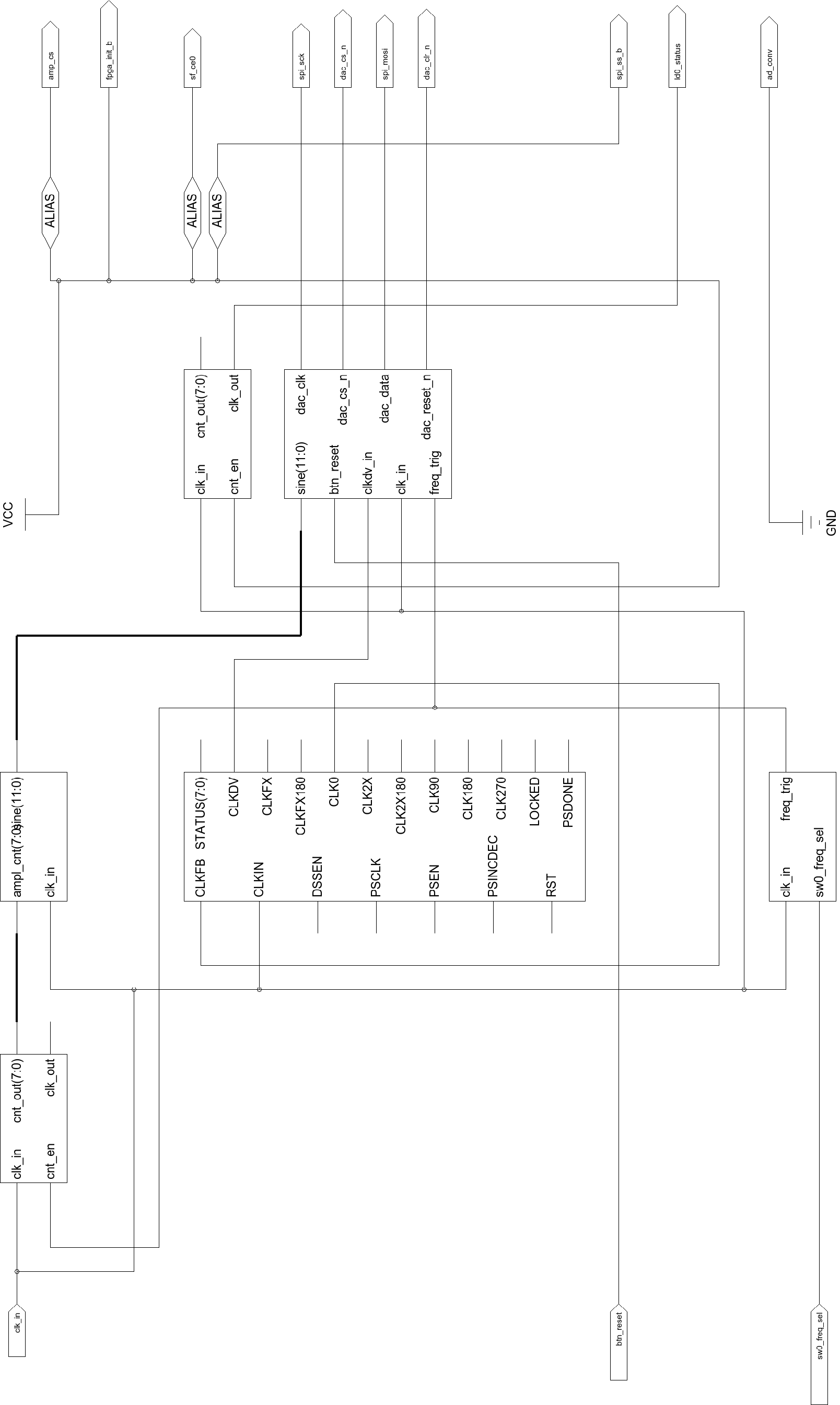
Illustration
9.1: Modulator RTL Detailed Schematic
9.2 Modulator Package
9.2.1 Description
Drawing
9.2.1: Package Description
Note:
used in dac_ltc2624_rtl.vhd
9.2.2 Create Module
modulator_pkg
code:
9.3 UCF-File
9.3.1 Description
9.3.2 Create Module
There are two different ways of
generating an ucf-file
For creating through the ISE Wizard
Select Project /
New Source
In the New Source dialog box,
select Implementation Constraints File, enter module_name_ucf
(modulator_rtl_ucf)
in the File name field an click Next
Click
Finish to open the
Constraint Timing Editor
Select
Ports in the
Constraint Type
window and insert the constraints like in the Illustration
Illustration
9.2: Constraint Timing Editor
Close
and Save Timing
Constraint Editor
For
creating through Text Editor
Open any text editor (for better usability
take one with vhdl code support)
Insert
the ucf constraints
Save
the file as module_name (e.g. modulation_rtl_ucf) into your
working directory
Change
the ending from *.txt
to *ucf
Optional: Launch
Project Navigator (if not
open)
Optional: Open
Project Modulator (modulator.ise)
(if not open)
In
the Project Navigator, select Project
/ Add Source
Select
module file (e.g.modulation_rtl_ucf.ucf)
Select
Implementation in
the Design View window
Click
Ok
ucf constraints:
NET "ad_conv"      LOC = "P11" | IOSTANDARD = LVCMOS33 | SLEW = SLOW | DRIVE = 6 ;
NET "amp_cs"       LOC = "N7"  | IOSTANDARD = LVCMOS33 | SLEW = SLOW | DRIVE = 6 ;
NET "btn_reset"    LOC = "V4"  | IOSTANDARD = LVTTL | PULLDOWN;
NET "clk_in"       LOC = "C9";
NET "dac_clr_n"    LOC = "P8"  | IOSTANDARD = LVCMOS33 | SLEW = SLOW | DRIVE = 8;
NET "dac_cs_n"     LOC = "N8"  | IOSTANDARD = LVCMOS33 | SLEW = SLOW | DRIVE = 8;
NET "fpga_init_b"  LOC = "T3"  | IOSTANDARD = LVCMOS33 | SLEW = SLOW | DRIVE = 4 ;
NET "ld0_status"   LOC = "F12";
NET "sf_ce0"       LOC = "D16" | IOSTANDARD = LVCMOS33 | DRIVE = 4 | SLEW = SLOW ;
NET "spi_mosi"     LOC = "T4"  | IOSTANDARD = LVCMOS33 | SLEW = SLOW | DRIVE = 8;
NET "spi_sck"      LOC = "U16" | IOSTANDARD = LVCMOS33 | SLEW = SLOW | DRIVE = 8;
NET "spi_ss_b"     LOC = "U3"  | IOSTANDARD = LVCMOS33 | SLEW = SLOW | DRIVE = 6 ;
NET "sw0_freq_sel" LOC = "L13" | IOSTANDARD = LVTTL | PULLUP;
9.4 Create Module
modulator_rtl
code:
library ieee;
    use ieee.math_real.all;
    use ieee.std_logic_1164.all;
    use ieee.std_logic_arith.all;
    use ieee.std_logic_textio.all;
    use ieee.std_logic_unsigned.all;
library std;
    use std.textio.all;
library unisim;
    use unisim.vcomponents.all;


entity modulator is
    generic(
        cntled_value_g  : std_logic_vector := x"ee6b27f"; -- clk counter led border
        cntampl_value_g : std_logic_vector := x"ff";      -- clk counter amplitude border
        depth_g         : integer range 1 to 99 := 8;     -- sine signal 8bit quantized
        freqhigh_g      : std_logic_vector (7 downto 0) := b"1100_0011"; -- threshold value of frequency a
        freqlow_g       : std_logic_vector (7 downto 0) := b"0011_0111"; -- threshold value of frequency b
        sim_g           : boolean := true;                     -- de- and activate dcm for simulation
        width_g         : integer range 1 to 99 := 12      -- 12 bit sine amplitude value
    );
    port(
        ad_conv      : out std_logic; -- default '0' set for error-free dac use
        amp_cs       : out std_logic; -- default '1' set for error-free dac use
        btn_reset    : in  std_logic; -- resetbutton
        clk_in       : in  std_logic; -- clk 50 MHz
        dac_clr_n    : out std_logic; -- dac reset (active low)
        dac_cs_n     : out std_logic; -- dac enable (active low)
        fpga_init_b  : out std_logic; -- default '1' set for error-free dac use
        ld0_status   : out std_logic; -- led clk (~0.5 Hz)
        sf_ce0       : out std_logic; -- default '1' set for error-free dac use
        spi_sck      : out std_logic; -- dac clk
        spi_mosi     : out std_logic; -- dac output
        spi_ss_b     : out std_logic; -- default '1' set for error-free dac use
        sw0_freq_sel : in  std_logic  -- frequency-select switch
    );
end;

architecture rtl of modulator is

    signal ampl_cnt_s  : std_logic_vector(depth_g-1 downto 0); -- amplitude counter
    signal sine_ampl_s : std_logic_vector(width_g-1 downto 0); -- amplitude counter
    signal clk0_s      : std_logic := '0';  -- 0 degree dcm clk output
    signal clkdv_s     : std_logic := '0';  -- divided clk (25 MHz)
    signal clk_in_s    : std_logic := '0';  -- clk (50 MHz)
    signal freq_trig_s : std_logic := '0';  -- frequency trigger

begin

dcm2sim_activation: if (sim_g) generate -- dcm activation

    dcm_sp_inst : dcm_sp
       generic map (
          clkdv_divide => 2.0    -- clk_in divided by 2.0
       )
       port map (
          clk0  => clk0_s,       -- 0 degree dcm clk output
          clkdv => clkdv_s,      -- divided dcm clk out (clkdv_divide)
          clkfb => clk0_s,       -- dcm clock feedback
          clkin => clk_in        -- clock input (from ibufg, bufg or dcm)
       );
end generate;

dcm2sim_deactivation: if not(sim_g) generate -- dcm deactivation

    clkdv_p: process
    begin

        wait until rising_edge(clk_in);
        clk_in_s <= not(clk_in_s); -- clk_in divided by 2

    end process;

    clkdv_s <= clk_in_s;

end generate;

counterled : entity work.counter(rtl) -- generate ~0,5Hz frequency for led
    generic map(
        cnt_value_g => cntled_value_g -- clk counter threshold value
    )
    port map (
        clk_in  => clk_in,
        clk_out => ld0_status,
        cnt_out => open,
        cnt_en  => '1'
    );

freq_ce : entity work.freq_ce(rtl) -- generate frequency trigger
    generic map(
        freqhigh_g => freqhigh_g,  -- clk counter threshold value
        freqlow_g  => freqlow_g    -- clk counter threshold value
    )
    port map(
        clk_in       => clk_in,
        freq_trig    => freq_trig_s,
        sw0_freq_sel => sw0_freq_sel
    );

counterampl : entity work.counter(rtl) -- generate amplitude values
    generic map(
        cnt_value_g => cntampl_value_g   -- clk counter threshold value
    )
    port map (
        clk_in  => clk_in,
        clk_out => open,
        cnt_out => ampl_cnt_s,
        cnt_en  => freq_trig_s
    );

sine : entity work.sine(rtl) -- generates digital sine
    generic map(
        depth_g => depth_g, -- sine signal 8bit quantized
        width_g => width_g  -- 12 bit sine amplitude value
    )
    port map(
        ampl_cnt  => ampl_cnt_s, -- amplitude counter
        clk_in    => clk_in,     -- 50MHz clock
        sine => sine_ampl_s      -- sine
    );

dac_ltc2624: entity work.dac_ltc2624(rtl) -- fetch freq-trigger and ampl-values and generate dac output signals
    generic map(
        depth_g => depth_g, -- sine signal 8bit quantized
        width_g => width_g  -- 12 bit sine amplitude value
    )
    port map(
        sine        => sine_ampl_s,
        btn_reset   => btn_reset,
        clk_in      => clk_in,
        clkdv_in    => clkdv_s,
        dac_clk     => spi_sck,
        dac_cs_n    => dac_cs_n,
        dac_data    => spi_mosi,
        dac_reset_n => dac_clr_n,
        freq_trig   => freq_trig_s
    );

ad_conv     <= '0'; -- default '0' set for error-free dac use
amp_cs      <= '1'; -- default '1' set for error-free dac use
fpga_init_b <= '1'; -- default '1' set for error-free dac use
sf_ce0      <= '1'; -- default '1' set for error-free dac use
spi_ss_b    <= '1'; -- default '1' set for error-free dac use

end;
9.5 Create Testbench
Note:
Other outputs have not to be simulated
Create
the modulator top testbench using the steps in chapter
3.2
with
modulator_rtl_tb.vhd
file name and the following code
modulator_rtl_tb
code:
library ieee;
    use ieee.std_logic_1164.all;
    use ieee.std_logic_arith.all;
    use ieee.std_logic_textio.all;
    use ieee.std_logic_unsigned.all;
library modelsim_lib;
    use modelsim_lib.util.all;
library std;
   use std.textio.all;

entity modulator_tb is
    generic(
        depth_g : integer range 0 to 99 := 8;  -- sine signal defaut 8bit quantized
        width_g : integer range 0 to 99 := 12; -- default 12 bit sine amplitude value
        write_mem2file_g : boolean := false    -- de- and aktivate generation of sin.txt
    );
end;

architecture tb of modulator_tb is

    constant per_c : time := 20 ns; -- clock period

    signal btn_reset_s     : std_logic := '0'; -- resetbutton
    signal clk_in_s        : std_logic := '1'; -- 50MHz clock
    signal dac_amplvalue_s : std_logic_vector (11 downto 0) := (others => '0'); -- amplidude value
    signal dac_clr_n_s     : std_logic := '1';
    signal dac_cs_n_s      : std_logic := '1'; -- dac enable (active low)
    signal freq_trig_s     : std_logic := '0'; -- frequency trigger
    signal ld0_status_s    : std_logic := '1'; -- led clk (~0.5 Hz)
    signal spi_mosi_s      : std_logic := '0'; -- dac output
    signal spi_sck_s       : std_logic := '1'; -- dac clk
    signal sw0_freq_sel_s  : std_logic := '1'; -- frequency-select switch
    signal wr_count_s      : integer range 0 to 64 := 0; -- write counter
    signal wr_end_s        : std_logic := '0'; -- write end

begin

    dut : entity work.modulator -- fetch generic and port of modulator_rtl.vhd
        generic map(
            depth_g => depth_g,
            width_g => width_g
        )
        port map(
            btn_reset    => btn_reset_s,
            clk_in       => clk_in_s,
            dac_clr_n    => dac_clr_n_s,
            dac_cs_n     => dac_cs_n_s,
            ld0_status   => ld0_status_s,
            spi_mosi     => spi_mosi_s,
            spi_sck      => spi_sck_s,
            sw0_freq_sel => sw0_freq_sel_s
       );

write_mem2file_gen: if (write_mem2file_g) generate -- generate first 64 following sin-amplitude values in sin.txt

    spy_init : process
    begin
        -- use dac_amplvalue_s signal of modulator_rtl
        init_signal_spy("/modulator_tb/dut/dac_amplvalue_s","/dac_amplvalue_s",0,1);
        -- use freq_trig_s signal of modulator_rtl
        init_signal_spy("/modulator_tb/dut/freq_trig_s","/freq_trig_s",0,1);
        wait;
    end process;

    write_p : process -- write 64 following sin-amplitude values in sin.txt at the work directory (only simulate)

        file out_sin_f : text open write_mode is "sin.txt"; -- create file in write mode in work directory

        variable out_sin_line_v : line; -- line variable

    begin

        wait until rising_edge(clk_in_s);

        if wr_end_s = '0' and freq_trig_s = '1' then
            if wr_count_s = 64 then -- write 64 amplitude values
                wr_end_s <= '1';    -- write end/end of file
            else
                write(out_sin_line_v, dac_amplvalue_s); -- write dac_amplvalue_s value in out_sin_line_v
                writeline(out_sin_f, out_sin_line_v);   -- write out_sin_line_v in one line of out_sin_f
                wr_count_s <= wr_count_s+1;             -- increment write counter
            end if;
        end if;

    end process;

end generate;

    clk_in_s  <=  not (clk_in_s) after per_c/2; -- generate 50MHz clock
    sw0_freq_sel_s <= '1', '0' after 25 us;     -- sw0_freq_sel high, low after variable time
    btn_reset_s    <= '1' after 50 us;          -- btn_reset high after 50 us

end;
9.6 Simulate
For using the write_mem2file_gen
part you have to use Modelsim.
Otherwise
comment:
library
std;
use std.textio.all;
library
unisim;
use unisim.vcomponents.all;
Choose your simulator:
Simulate 80 μs
Assuming no errors, your
simulation result should look similar to Illustration
Illustration
9.3: Simulate Modulator RTL
9.7 Generate Programming File
9.7.1 Description
The Generate Programming File process
produces a bitstream for Xilinx device configuration. After the
design is completely routed, you must configure the device so it can
execute the desired function.
In the Sources window,
right-click on the programming module (modulator_rtl)
and select Set as Top Module,
if not set
In
the Sources window, select programming module
(modulator_rtl).
In Process window double-click Generate Programming File
(see Illustration )
Illustration
9.4: Generate Programming File Modulator RTL
9.7.2 Programming File Generation Report
Shows an summary of chosen Bitgen
options
9.8 Configure Target Device
Note: For only programming the
design into the volatile flash memory of the FPGA, start
iMPACT and program generated bit-file through JTAG
9.8.1 Generate Target PROM/ACE File
In the
Sources window, select programming
module (modulator_rtl).
In Process window, expand Configure Target Device and double-click
Generate Target PROM/ACE
File
Select
Prepare a PROM File
and click Next
Type
in file name
(modulator)
in the PROM File Name
field, click Next
– Next
Select
Auto Select PROM (for
beginners), click Next
Click
Finish
Open
the Programming File
(modulator.bit)
Select
Prepare a System ACE
File
and click Next
Click
Next
– Next (or
change if required)
Type
in file name
(modulator)
in the Name
field,
click Next
Assign
a Configuration Address
and rename (if required)– Click Next
Click
Finish
Open
the Programming File
(modulator.bit)
9.8.2 Manage Configuration Project (iMPACT)
Opens a wizard for programming via
JTAG, PROM, Boundary-Scan File and through different modes
9.9 Programming
Instead of programming the device
following the steps of 8.8 Configure Target Device,
you can start iMPACT independently
Connect the JTAG download
cable
Power on the Spartan 3e
Demoboard
Launch iMPACT
Click
Cancel (do not open
an existing project)
Double-click on Boundary-Scan
Right-Click
in the Boundary window / Initialize JTAG chain
Verify that iMPACT found the
device
Illustration
9.5.: Boundary Scan
Assign the binary design file
(e.g. *.bit) - modulator.bit from your working
directory into the volatile memory, click Open
Optional:
Assign the binary design file (e.g. *.mcs) from your working
directory into the non-volatile memory, click Open – else
click Bypass
Optional:
Assign the binary design file (e.g. *.jed) from your working
directory into the onboard CPLD, click Open – else click
Bypass
Click
Ok, or change Device Programming Properties if required
Right-click
on the programming device ( device which displays the
modulator.bit file) / Programm, will load your design
into the device
Assuming
no errors occurs, you can test your design with a chipscope core
(see 8.10 Chipscope) or an oscilloscope (see 8.11
Oscilloscope)
9.10 Chipscope
9.10.1 Description
On-chip debugging: integrated
logic analyzer (ILA), integrated bus analyzer (IBA), and virtual
input/output (VIO) low-profile software cores.
Allow you to view internal
signals and nodes in your FPGA
ChipScope Pro cores:
ILA: The ILA core is a
customizable logic analyzer core that can be used to monitor the
internal signals in your design. Because the ILA core is
synchronous to the design being monitored, all design clock
constraints applied to your design are also applied to the
components inside the ILA core.
ATC2: The Agilent Trace
Core 2 (ATC2) is a customizable logic analyzer core, which is not
included in the standard ISE (shareware) and is similar to the ILA
core but does not use on-chip Block RAM resources to store captured
trace data. The ATC2 core synchronizes ChipScope Pro to the Agilent
FPGA dynamic probe technology, delivering the first integrated
application for FPGA debug with an external logic analyzers.
Note:
EDK
provides additional specific cores.
9.10.2 Create a ChipScope
core
Select
Project /
New Source
In
the New Source dialog box, select ChipScope
Definition and File, enter
chipscope_name
(modulator)
in the File name field an click Next
Select
analysing source
file
(modulator)
Click
Finish
Double-Click
on the chipscope file (modulator.cdc)
in the “Sources for” window to start the ChipScope Pro Core
Inserter
Click
Next
(or
change if required)
Select New ILA Unit in
the ChipScope Pro Core Inserter after the steps in 8.10.2
Create a
ChipScope core
Click
on the ILA
module above the core utilization window to modify the core
Set
Trigger
Width
in the Trigger Parameters Tab to 5
Select
Modify
Connections
in the Net Connections Tab
Select
clk_in_IBUFG
as clock signal and click Make
Connections (see
Illustration)
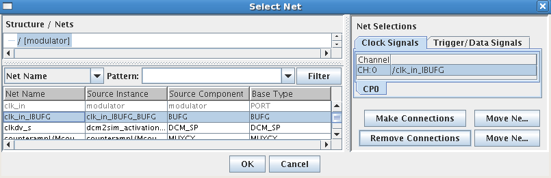
Illustration
9.6: ILA Clock Signals
Select
Trigger/Data
Signals
Tab in the Net Selection Tab
Make
following connections (see Illustration)
clk_out_s
dac_clk_s
dac_cs_n_s
dac_out_serial_s
dac_reset_n
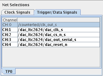
Illustration
9.7: ILA Trigger/Data Signals
Close
and Save
ChipScope Pro Core Inserter
Rerun
Generate Programming File (see 8.7
Generate Programming File)
Configurate
Device (see 8.9
Programming)
Select New ATC2
Unit in the ChipScope Pro Core Inserter after the steps in
8.10.2 Create
a ChipScope core
Click
on the ATC2
module above the core utilization window to modify the core
Set
ATD
Pin Count
in the Pin Selection Parameters Tab to 5 (see next Illustration)
Set
following pin settings (see Illustration)
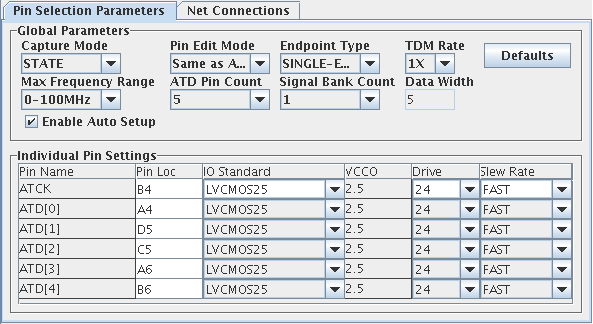
Illustration
9.8: ATC2 Pin Selection Parameters
Select
Modify
Connections
in the Net Connections Tab
Modify
it like for an ILA core (see 8.10.3
ILA
- step
5-7)
Close
and
Save
ChipScope Pro Core Inserter
Rerun
Generate Programming File (see 8.7
Generate Programming File)
Configurate
Device (see 8.9
Programming)
9.10.3 Analyze a
ChipScope core
In the
Sources window, click on the analyzable
module (modulator_rtl)
, double-click Analyze Design Using Chipscope
in the Process window
Click
on the icon Open Cable/Search JTAG Chain
Note:
Verify that your design is running
Click
Ok
Select
Trigger Setup / Run
Now
you should see your design being analyed by the onboard chipscope
module.
Shift
the switch (sw0) to the other position
Rerun
(Select Trigger Setup / Run)
Note:
More Settings see in the ISE help.
9.11 Oscilloscope
To see the analog sine from the DAC
you have to analyze you design with an oscilloscope
Programm design (see 8.9
Programming)
Connect the probe from the
Oscilloscope to the A output channel of the LTC2624 Quad DAC
(see Illustration)
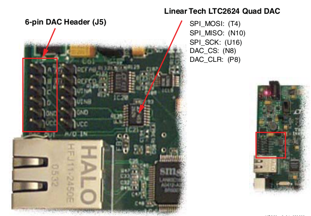
Illustration
9.9.: DAC Connections
Note: Do not forget to
connect your probe ground wire to the ground pin of the DAC
Now, if your oscilloscope
settings are correct (click Autoset), you should see a sine
signal on the display
Shift
the switch (sw0) to the other position to see the signal with an
other frequency