|

|
All right
strictly reserved. Reproduction or issue to third parties, in
any form whatsoever, is not permitted without written authority
from the proprietors.
|
VHDL Style Guide
|
|
Project
Name/Projektname
|
Page/Seite
|
|
|
of/von
5
|
|
Prepared
/ Erstellt
|
Subject
Responsible / Verantwortlich
|
Date/Datum
|
Rev.
|
File/Datei
OpenOffice.org Writer
|
|
Mario
Fohler
|
Peter
Thorwartl
|
2008-07-31
|
1.0
|
|
1. General Coding Rules for Digital
Designs
1.1 Reset
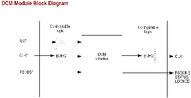
1.2 Clocks
entity
modulator is
generic(
...
);
port(
clk_in
: in std_logic; -- clk 50 MHz
...
);
end;
architecture
rtl of modulator is
...
begin
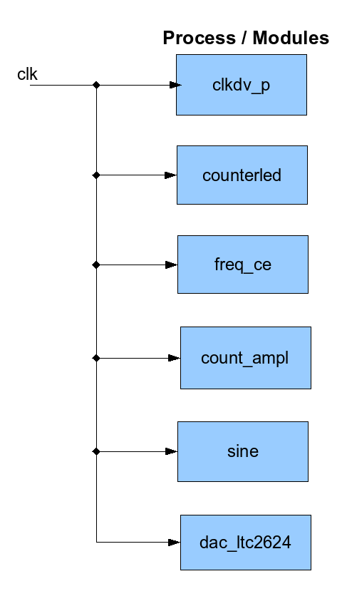
dcm2sim_activation:
if (sim_g) generate -- dcm
activation
...
end
generate;
dcm2sim_deactivation:
if not(sim_g) generate -- dcm
deactivation
clkdv_p:
process
begin
wait
until rising_edge(clk_in);
clk_in_s
<= not(clk_in_s); -- clk_in divided
by 2
end
process;
clkdv_s
<= clk_in_s;
end
generate;
counterled
: entity work.counter(rtl) -- generate
~0,5Hz frequency for led
generic
map(
clkcnt_value_g
=> x"2faf07f" -- clk counter
threshold value
)
port
map (
clk_in
=> clk_in,
...
);
freq_ce
: entity work.freq_ce(rtl) -- generate
frequency trigger
generic
map(
...
)
port
map(
clk_in
=> clk_in,
...
);
counterampl
: entity work.counter(rtl) -- generate
amplitude values
generic
map(
clkcnt_value_g
=> x"00000ff" -- clk counter
threshold value
)
port
map (
clk_in
=> clk_in,
...
);
sine
: entity work.sine(rtl) –- generates
digital sine
generic
map(
...
)
port
map(
...
clk_in
=> clk_in,
...
);
dac_ltc2624:
entity work.dac_ltc2624(rtl) -- fetch
freq-trigger and ampl-values and generate dac output signals
generic
map(
...
)
....port
map(
...
clk_in
=> clk_in,
...
);
...
end;
Do not use gated clocks.
No
internal clk-generation in moduls
Avoid using latches.
Do not use buffer as delay
elements.
All blocks external IOs should
be registered.
Avoid using both clock edges.
Clock signal must be connected
to global dedicated routing resources.
Do not use clocks or reset as
data or as enable.
Do not use data as clock or a
reset.
Signals that cross-different
clock domains should be sampled before and after crossing
domains (double sampling is preferred to minimize meta-stability).
Use
the lowest possible clock speed in each clock domain.
Use
the minimum number of clock domains
Use
clock enables
Example:
(counter_rtl)
entity
counter is
generic(
...
);
port(
...
cnt_en
: in std_logic -- clk counter
enable
);
end;
architecture
rtl of counter is
...
begin
counter_p:
process
begin
wait
until rising_edge(clk_in);
if
(cnt_en = '1') then
...
else
...
end
if;
end
process;
...
end;
Clock enables can only be inferred in
a clocked process.
Clock enables can be inferred
explicitly by testing an enable signal. If the enable is true, the
signal is updated. If enable is false, that signal will hold its
current value.
Clock enables can be implicitly
inferred two ways:
Not assigning to a signal in every
branch of an if-then-else statement or case statement. Remember that
latches will be inferred for this condition in a combinatorial
process
Not
defining all possible states or branches of an if-then-else or case
statement.
1.3 Buses
Start buses at the LSB.
Use MSB to LSB for data buses.
Use LSB to MSB for delay lines
and shift registers.
Start counting with one
Avoid using internal tri-state
signals, they no longer exist on FPGAs. The will be modelled with
two buses, one for reading and one for writing.
1.4 Finite State Machine FSM
Generally, use three process
statements for a state machine: one process for next-state decoding,
one for output decoding, and one for the registering of state bits
and outputs.
Use a Mealy look-ahead state machine
with registered outputs whenever possible, or use a Moore state
machine with next-state output decoding and registered outputs to
incur the minimum amount of latency.
Use enumeration types
for the states
Use one hot encoding for FPGAs
Use binary, gray, sequential
coding for CPLDs
Example:
(statemachine_rtl)
entity
statemachine is
port(
clk_in
: in std_logic; -- 50MHz clock
dac_clk_low
: out std_logic; -- set dac clk to zero
shreg_en
: out std_logic; -- shiftregister
enable
statem_en
: in std_logic -- statemachine
enable
);
end;
architecture
rtl of statemachine is
type
state_type_t_enum is (shreg_end,shreg_start,clk_pause); --
three states of state machine
signal
dac_clk_low_s : std_logic := '0'; --
set dac clk low
signal
shreg_en_s : std_logic := '0'; -- set shiftreg enable low
signal
statem_loop_s : integer range 0 to 49 := 0; --
state loop
signal
statem_s : state_type_t_enum; --
enumerated state machine
begin
statem_statereg_p
: process -- shift states
begin
wait
until rising_edge(clk_in);
if
((statem_en = '1') or (dac_clk_low_s = '1')) then
case
statem_s is
when
shreg_end =>
statem_s
<= shreg_start;
when
shreg_start =>
if
(statem_loop_s = 48) then
statem_s
<= clk_pause;
statem_loop_s
<= 0;
else
statem_loop_s
<= statem_loop_s + 1;
end
if;
when
clk_pause =>
if
(statem_loop_s = 1) then
statem_s
<= shreg_end;
statem_loop_s
<= 0;
else
statem_loop_s
<= statem_loop_s + 1;
end
if;
when
others => null;
end
case;
end
if;
end
process;
statem_stateoutput_p
: process(statem_s) -- define output to
state
begin
case
statem_s is -- generate shiftregister enable
and clk output low signal
when
shreg_start =>
shreg_en_s
<= '1'; -- start shift register
dac_clk_low_s
<= '0';
when
clk_pause =>
shreg_en_s
<= '0'; -- end shift register
dac_clk_low_s
<= '1'; -- set dac clk low
when
shreg_end =>
shreg_en_s
<= '0';
dac_clk_low_s
<= '0';
when
others => null;
end
case;
end
process;
shreg_en
<= shreg_en_s;
dac_clk_low
<= dac_clk_low_s;
end;
1.5 Memories
--
8x32 lut-matrix
type
lut8x32_t_arr is
array
(0 to
31) of
std_logic_vector(7
downto
0);
--
8bit amplitude values of 32bit quantized sin
constant
wave_c : lut8x32_t_arr := (
0
=> X"8C", 1 => X"A5", 2 => X"BC",
3 => X"D0",
4
=> X"E2", 5 => X"F0", 6 => X"FA",
7 => X"FE",
8
=> X"FE", 9 => X"FA", 10 => X"F0",
11 => X"E2",
12
=> X"D0", 13 => X"BC", 14 => X"A5",
15 => X"8C",
16
=> X"73", 17 => X"5A", 18 => X"43",
19 => X"2F",
20
=> X"1D", 21 => X"0F", 22 => X"05",
23 => X"01",
24
=> X"01", 25 => X"05", 26 => X"0F",
27 => X"1D",
28
=> X"2F", 29 => X"43", 30 => X"5A",
31 => X"73"
);