1. INTRODUCTION
1.1 Motivation
Basic FPGA Tutorial is a document made for beginners who are entering the FPGA world. This tutorial explains, step by step, the procedure of designing a simple digital system using VHDL language and Xilinx design tools.
1.2 Purpose of this tutorial
This tutorial is made to introduce you how to create, simulate and test an project and run it on your development board.
After completing this tutorial, you will be able to:
- Launch and navigate the Project Navigator
- Locate and insert snippets from the Language Templates
- Demonstrate the capabilities of the text editor
- Simulate a design using integrated Simulator ISim
- Run your design on the target development board
- Debug a design in hardware using ChipScope Pro Tool and Oscilloscope
The following project is designed for:
- Designing Surface: ISE 14.7
- HD Language: VHDL
- Simulator: ISIM
- Device: Xilinx Kintex-7 KC705 Development Board
1.3 Objectives of this tutorial
In this tutorial a PWM signal modulated using the sine wave with two different frequencies (1 Hz and 3.5 Hz) will be created. Frequency that will be chosen depends on the position of the two-state on-board switch (sw0).
PWM Signal
Pulse-width modulation (PWM) uses a rectangular pulse wave whose pulse width is modulated by some other signal (in our case we will use a sine wave) resulting in the variation of the average value of the waveform. Typically, PWM signals are used to either convey information over a communications channel or control the amount of power sent to a load. To learn more about PWM signals, please visit http://en.wikipedia.org/wiki/Pulse-width_modulation.
Drawing 1.1. illustrates the principle of pulse-width modulation. In this picture an arbitrary signal is used to modulate the PWM signal, but in our case sine wave signal will be used.
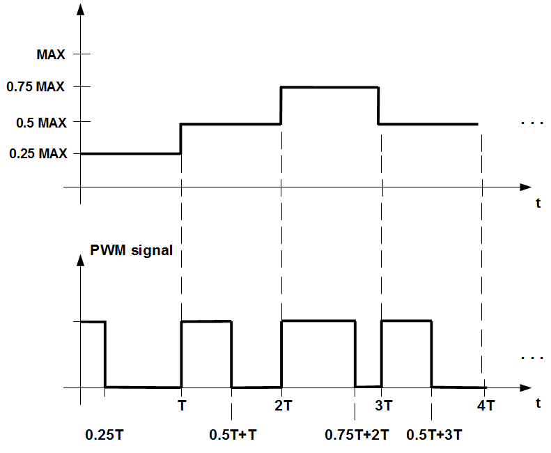
Drawing 1.1: Example of the PWM signal
1.4 One possible solution for the modulator design
Considering that we are working with digital systems and signals, our task will be to generate an digital representation of an analog (sine) signal with two frequencies: 1 Hz and 3.5 Hz.
Drawing 1.2 is showing the sine wave that will be used to modulate the PWM signal.
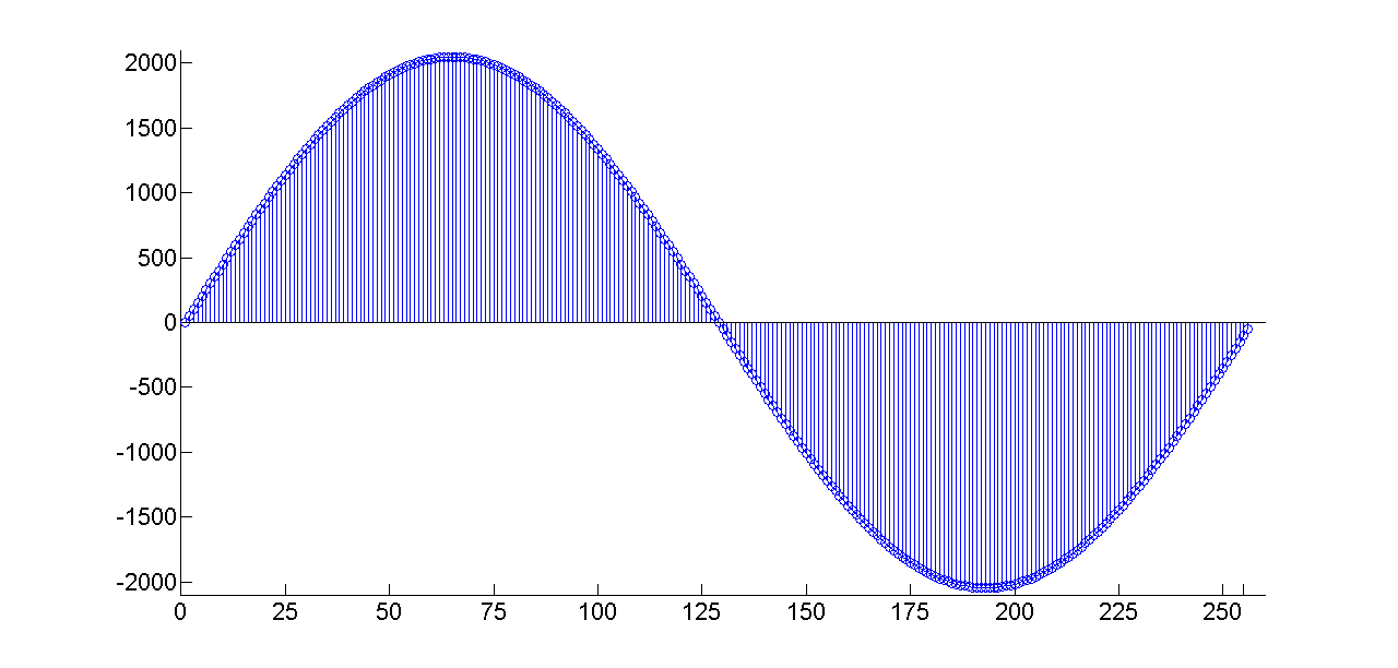
Drawing 1.2: Sine wave with 256 samples
One period of the sine wave is represented with 256 (28) samples, where each sample can take one of 4096 (212) possible values. Since the sine wave is a periodic signal, we only need to store samples of one period of the signal.
Note: Pay attention that all of sine signals with the same amplitude, regardless their frequency, look the same during the one period of a signal. The only thing that is different between those sine signals is duration of a signal period. This means that the sample rate of those signals is different.
Considering that the whole system will be clocked with the 200 MHz input signal, which is typically available on the new development boards, to get 1 Hz and 3.5 Hz frequencies (which is much smaller than 200 MHz) we should divide input clock frequency with integer value N.
In the Tables 1.1 and 1.2 are shown parameters that are necessary for generating sine signals with 1 Hz and 3.5 Hz frequencies.
Table 1.1: Sine signal with the frequency of 1 Hz
|
T=1 s |
T=1/1 Hz=1 s
|
T is the period of the signal |
|
f1=256 Hz |
f1=256*1 Hz=256 Hz (or read in time: 1 s/256)
|
f1 is the frequency of reading whole period (T) with 256 samples |
|
N1=781250 |
N1=200 MHz/256 Hz=781250
|
N1 is the number which divides frequency of the input clock signal (200 MHz) to the required frequency for the digital sine module |
|
N2=191 |
N2=781250/4096=190.73486 |
N2 is the number which divides frequency of the input clock signal (200 MHz) to the required frequency for the PWM's FSM module |
|
N1=782336 |
N1=191*4096=782336 |
This is new calculation, because N1 must be divisible with 4096 |
Table 1.2: Sine signal with the frequency of 3.5 Hz
|
T=0.286 s |
T=1/3.5 Hz=0.286 s
|
T is the period of the signal |
|
f2=896 Hz |
f2=256*3.5 Hz=896 Hz (or read in time: 0.286 s/256)
|
f2 is the frequency of reading whole period (T) |
|
N1=223214 |
N1=200 MHz/896 Hz=223214.2857
|
N1 is the number which divides frequency of the input clock signal (200 MHz) to the required frequency |
|
N2=54 |
N2=223214/4096=54.4956 |
N2 is the number which divides frequency of the input clock signal (200 MHz) to the required frequency for the PWM's FSM module |
|
N1=221184 |
N1=54*4096=221184 |
This is new calculation, because N1 must be divisible with 4096 |
Now, it is obvious that the sine wave can be generated by reading sample values of one period, that are stored in one table, with appropriate speed. In our case the values will be generated using the sine function from the IEEE Math library and will be stored in an ROM memory.
Note: All of these information, such as what is the purpose of this tutorial, explanation what is the PWM signal, frequency calculations and block diagram as one possible solution for the modulator design, are illustrated in the Lab 1: ”Introduction”.
Block diagram
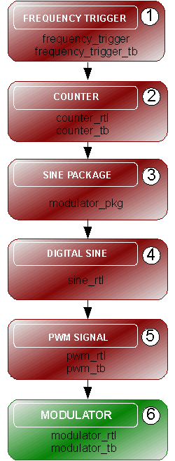
Block diagram on the Drawing 1.3 shows the structure of one possible system that can be used to generate required PWM signals.
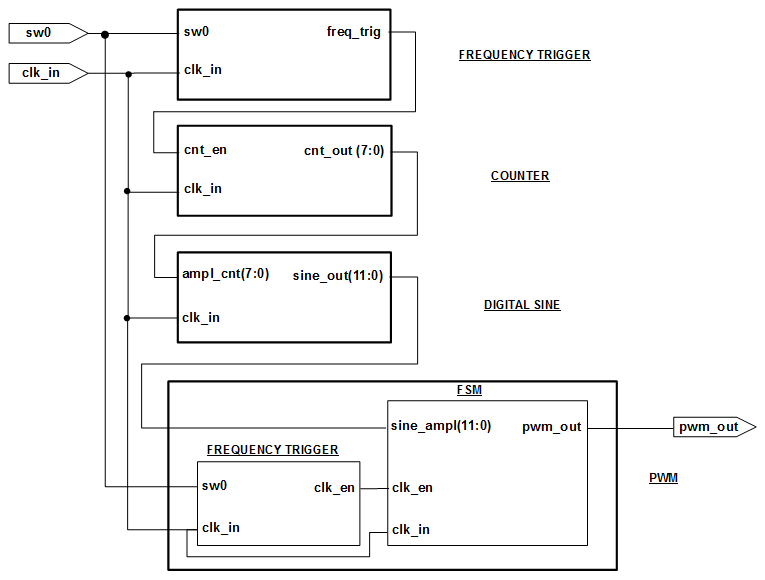
Drawing 1.3: Block diagram
Let us briefly explain each module shown on the Drawing 1.3:
- Frequency Trigger
- Counter
- Digital Sine
- PWM
-
- First we will create the Frequency Trigger module that will provide one output signal with two possible frequencies
- Then, we will create the Counter module, that will generate read addresses for the ROM where samples of the sine wave will be stored
- Then we will create an VHDL package with a parametrized sine signal
- After that, we will make the Digital Sine module, where we will generate an digital representation of an analog (sine) signal and where we will include the Sine package
- After that, we will generate PWM signal with the PWM module
- At the end, we will create Modulator module where we will merge all the previously designed modules into one big design.
- Design Entry – the first step in creating a new design is to specify it's structure and functionality. This can be done either by writing an HDL model using some text editor or drawing a schematic diagram using schematic editor.
- Design Synthesis – next step in the design process is to transform design specification into a more suitable representation that can be further processed in the later stages in the design flow. This representation is called the netlist. Prior to netlist creation synthesis tool checks the model syntax and analyse the hierarchy of your design which ensures that your design is optimized for the design architecture you have selected. The resulting netlist is saved to an Native Generic Circuit (NGC) file (for Xilinx® Synthesis Technology (XST) compiler) or an Electronic Design Interchange Format (EDIF) file (for Precision, or Synplify/Synplify Pro tools).
- Design Implementation
-
3.1 Translate step – merges all incoming netlists and constraints into a Xilinx Native Generic Database (NGD) file.
3.2 Map step - maps the design, specified by an NGD file, into available resources on the target FPGA device, such as LUTs, Flip-Flops, BRAMs,... As a result, an Native Circuit Description (NCD) file is created.
3.3 Place and Route step - takes a mapped Native Circuit Description (NCD) file, places and routes the design, and produces an NCD file that is used as input for bitstream generation.
-
Design Verification – is very important step in design process. A verification is comprised of seeking out problems in the HDL implementation in order to make it compliant with the design specification. A verification process reduces to extensive simulation of the HDL code. Design Verification is usually performed using two approaches: Simulation and Static Timing Analysis.
There are two types of simulation:
- Functional (Behavioral) Simulation – enables you to simulate or verify a code syntax and functional capabilities of your design. This type of simulation tests your design decisions before the design is implemented and allows you to make any necessary changes early in the design process. In functional (behavioral) simulation no timing information is provided.
-
Timing Simulation – allows you to check does the implemented design meet all functional and timing requirements and behaves as you expected. The timing simulation uses the detailed information about the signal delays as they pass through various logic and memory components and travel over connecting wires. Using this information it is possible to accurately simulate the behaviour of the implemented design. This type of simulation is performed after the design has been placed and routed for the target PLD, because accurate signal delay information can now be estimated. A process of relating accurate timing information with simulation model of the implemented design is called Back-Annotation.
-
Static Timing Analysis – helps you to perform a detailed timing analysis on mapped, placed only or placed and routed FPGA design. This analysis can be useful in evaluating timing performance of the logic paths, especially if your design doesn't meet timing requirements. This method doesn't require any type of simulation.
-
Generate Programming File – this option runs BitGen, the Xilinx bitstream generation program, to create a bitstream file that can be downloaded to the device.
- Programming – iMPACT Programmer uses the output from the Generate Programming File process to configure your target device.
-
Testing – after configuring your device, you can debug your FPGA design using the Xilinx ChipScope Pro tool or some external logic analyzer.
- Estimate Power – after implementation, you can use the XPower Analyzer for estimation and power analysis. XPower Analyzer is delivered with ISE Design Suite. With this tool you can estimate power, based on the logic and routing resources of the actual design.
This module will generate one output signal with two possible frequencies calculated in the Tables 1.1 and 1.2, one with 256 Hz and the second one with 896 Hz. Which frequency will be chosen depends on the position of the two-state on-board switch (sw0).
This module will be an universal (generic) counter. It's task will be to generate read addresses for the ROM where samples of the sine wave are stored. The speed of the counting will be controlled by the Frequency Trigger module, via freg_trig port, and the output of the Counter module will be an input of the Digital Sine module.
This module will generate an digital representation of an analog (sine) signal with desired frequency. It will use the counter values as addresses to fetch the next value of the sine wave from the ROM.
In our case we will make an VHDL package with a parametrized sine signal. 28=256 unsigned amplitude values during one sine-period that will be stored into an ROM array.
VHDL package is a way of grouping related declarations that serve a common purpose. Each VHDL package contains package declaration and package body.
Note: Don't forget to include the Sine package in the code of the Digital Sine module !
This module will generate an PWM signal modulated using the digital sine wave from the Digital Sine module. This module will be composed of two independent modules. One will be the Frequency Trigger, for generating two different frequencies and the second one will be the Finite State Machine (FSM), for generating the PWM signal.
Frequency Trigger – output from this module will be used to control the frequency at which FSM module works. As we have already said, in PWM signal information is represented as duty cycle value in each period of the signal. Since our digital sine signal can have 4096 possible values, there will also be 4096 different duty cycle values. This means that PWM's FSM must operate at frequency that is 4096 times higher than the one used by the Digital Sine module.
FSM – is necessary to generate the PWM signal. It will generate the PWM signal with correct duty cycle for each period based on the current amplitude value of digital sine signal, that is stored in the ROM.
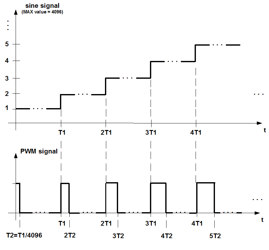
Drawing 1.4: Details of PWM signal generation
Note: In the Lab 2: “Using the Tools” is illustrated the structure and the interface of this project, which modules we will have in our design and what will be our design steps.
Design steps
This tutorial will be realized step by step with the idea to explain the whole procedure of designing an digital system.
On the Drawing 1.5 are shown steps in designing modules of this lab:
Drawing 1.5: Project Design Steps
1.5 Design Flow
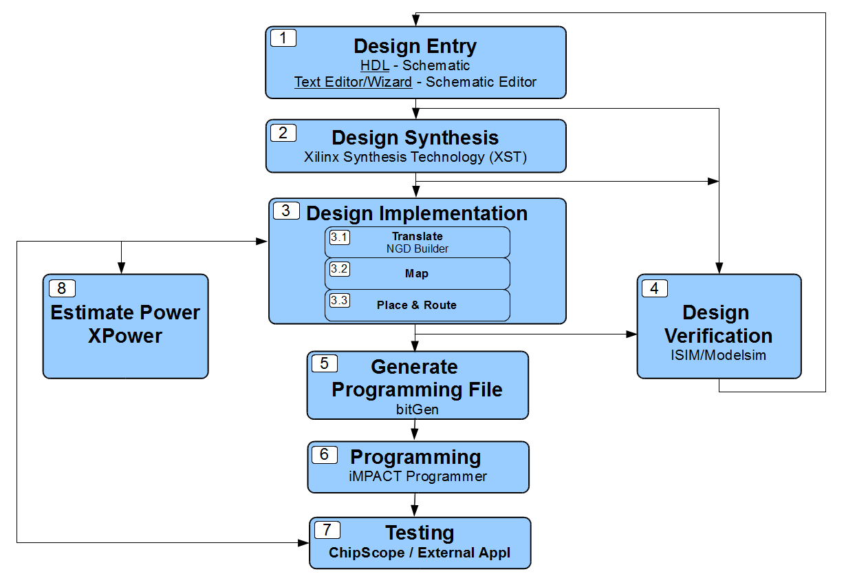
Drawing 1.6: Design Flow
Implementation step maps netlist produced by the synthesis tool onto particular device's internal structure. It consists from three steps:
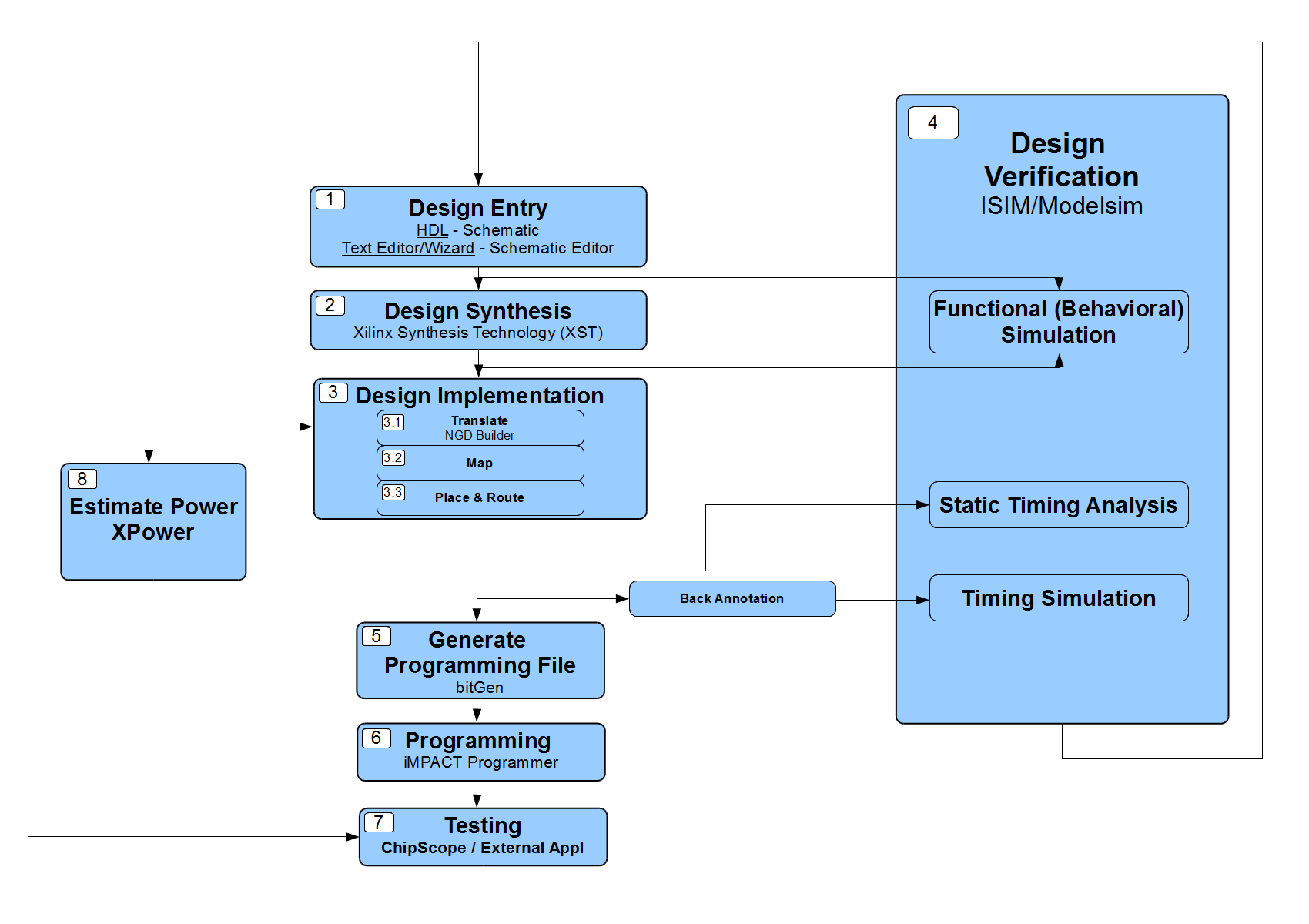
Drawing 1.7: Design Verification Steps
Note: In the Lab 2: “Using the Tools” you can also find a short description about Design Synthesis and Design Implementation (Translation, Map and Place&Route).