6. DIGITAL SINE TOP
6.1 Description
- Usage: This module will merge Frequency Trigger, Counter, Sine package and Digital Sine module into one Digital Sine Top module (Drawings 6.1 and 6.2). It will have two input ports: one will be used for input clock signal (clk_in) and the second one will be used for changing output signal frequency (sw0). The only output port will represent the current amplitude value of the desired sine signal.
- Block diagram:
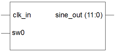
Drawing 6.1: Digital Sine Top block diagram
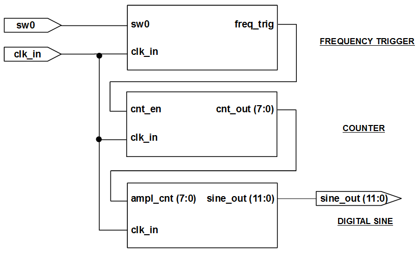
Drawing 6.2: Digital Sine Top detailed block diagram
- Input ports:
- clk_in: input clock signal
- sw0: input signal from the on-board switch, used for changing output signal frequency
- Output ports:
- sine_out: current amplitude value of the sine signal
- Generics:
- cnt_value_g: threshold value for counter, it's value should be equal to (2^depth)-1
- depth_g: the number of samples in one period of the signal
- width_g: the number of bits used to represent amplitude value
- div_factor_freqhigh_g: threshold value of frequency a
- div_factor_freqhigh_g: threshold value of frequency b
- File name: sine_top_rtl.vhd
6.2 Creating Module
To create Digital Sine Top module, use steps for creating modules, Sub-chapter 2.3.1 Creating a Module Using an Text Editor.
Digital Sine Top VHDL model:
library ieee;
use ieee.std_logic_1164.all;
use ieee.std_logic_arith.all;
use ieee.std_logic_unsigned.all;
use work.modulator_pkg.all;
entity sine_top is
generic(
cntampl_value_g : integer := 255; -- threshold value for counter, it's value should be equal to (2^depth)-1
depth_g : integer range 1 to 99 := 8; -- the number of samples in one period of the signal
width_g : integer range 1 to 99 := 12; -- the number of bits used to represent amplitude value
div_factor_freqhigh_g : integer := 57344; -- threshold value of frequency a
div_factor_freqlow_g : integer := 196608 -- threshold value of frequency b
);
port(
clk_in : in std_logic; -- input clock signal
sine_out : out std_logic_vector(width_g-1 downto 0); -- current amplitude value of the sine signal
sw0 : in std_logic -- signal used for selecting frequency
);
end;
architecture rtl of sine_top is
constant sin_ampl_c : vector_t_arr := init_sin_f(depth_g, width_g); -- returns sine amplitude value
signal ampl_cnt_s : std_logic_vector(depth_g-1 downto 0) := (others=>'0'); -- amplitude counter
signal freq_trig_s : std_logic := '0';
begin
counterampl : entity work.counter(rtl) -- counter instance
generic map(
cnt_value_g => cntampl_value_g,
depth_g => depth_g
)
port map (
clk_in => clk_in,
cnt_en => freq_trig_s,
cnt_out => ampl_cnt_s
);
freq_ce : entity work.frequency_trigger(rtl) -- frequency trigger instance
generic map(
div_factor_freqhigh_g => div_factor_freqhigh_g,
div_factor_freqlow_g => div_factor_freqlow_g
)
port map(
clk_in => clk_in,
freq_trig => freq_trig_s,
sw0 => sw0
);
sine : entity work.sine(rtl) -- digital sine instance
generic map(
depth_g => depth_g,
width_g => width_g
)
- port map(
ampl_cnt => ampl_cnt_s,
clk_in => clk_in,
sine_out => sine_out
);
end;
6.3 Creating Test Bench
- Usage: used to verify correct operation of the sine_top module defined in the sine_top_rtl.vhd file
- Test bench internal signals:
- clk_in_s: input clock signal
- sw0_s: input signal from the on-board switch, used for changing output signal frequency
- sine_out_s: current amplitude value of the sine signal
- Generics:
- cntampl_value_g: threshold value for counter
- depth_g: the number of samples in one period of the signal
- width_g: the number of bits used to represent amplitude value
- div_factor_freqhigh_g: threshold value of frequency a
- div_factor_freqlow_g: threshold value of frequency b
- File name: sine_top_tb.vhd
We will now create a test bench for Digital Sine Top module (sine_top_tb.vhd). We will use the same steps as for creating frequency_trigger_rtl.vhd module, explained in Sub-chapter 2.3.1 Creating a Module Using an Text Editor.
library ieee;
use ieee.std_logic_1164.all;
use ieee.std_logic_arith.all;
use ieee.std_logic_unsigned.all;
use work.modulator_pkg.all;
entity sine_top_tb is
generic(
cntampl_value_g : integer := 255; -- threshold value for counter, it's value should be equal to (2^depth)-1
depth_g : integer range 1 to 99 := 8; -- the number of samples in one period of the signal
width_g : integer range 1 to 99 := 12 -- the number of bits used to represent amplitude value
div_factor_freqhigh_g : integer := 55; -- threshold value of frequency a
div_factor_freqlow_g : integer := 195; -- threshold value of frequency b
);
end;
architecture tb of sine_top_tb is
signal clk_in_s : std_logic := '0'; -- input clock signal
signal sine_out_s : std_logic_vector(width_g-1 downto 0) := (others=>'0'); -- current amplitude value of the sine signal
signal sw0_s : std_logic := '0'; -- signal used for selecting frequency
begin
dut : entity work.sine_top -- sine_top instance
generic map(
cntampl_value_g => cntampl_value_g,
depth_g => depth_g,
width_g => width_g,
div_factor_freqhigh_g => div_factor_freqhigh_g,
div_factor_freqlow_g => div_factor_freqlow_g
)
port map(
clk_in => clk_in_s,
sine_out => sine_out_s,
sw0 => sw0_s
);
clk_in_s <= not (clk_in_s) after per_c/2; -- 50 MHz input clock signal
sw0_s <= '0', '1' after 1 ms;
end;
6.4 Simulating
After you have entered the code for the input stimulus in order to perform simulation:
- You can start your simulation (see Chapter 3.4 Simulating)
- Simulate your design for 4 ms (see Chapter 2.5 Simulating – step 12.)
- Assuming no errors, your simulation result should look similar to Illustration 6.1.
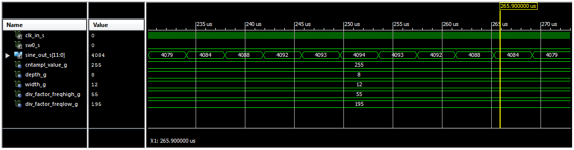
Illustration 6.1 Simulation Results
Note: Information about creating the Digital Sine Top Module, generating its test bench and simulating the Digital Sine Top design, you can also find in the Lab 8: “Creating Digital Sine Top Module”.
6.5 Synthesize
6.5.1 Description
-
Synthesis is the process of transforming an RTL-specified design into a gate-level representation. It checks code syntax and analyse the hierarchy of your design. This ensures that your design is optimized for the design architecture that you have selected (e.g. Number of Flip-Flops, LUTs, Clock- and IO-Buffers). The resulting netlist is saved to an Native Generic Circuit (NGC) file (for Xilinx® Synthesis Technology (XST) compiler) or an Electronic Design Interchange Format (EDIF) file (for Precision, or Synplify/Synplify Pro tools).
6.5.2 Synthesize
To synthesize your design, follow these steps:
- In the Design window, select Implementation view
- In the Hierarchy window, right-click on the synthesizable module (sine_top - rtl) and select Set as Top Module, if it is not already set
- In the Hierarchy window, select synthesizable module (sine_top – rtl) and in the Processes window, double-click on the Synthesize – XST command, see Illustration 6.2
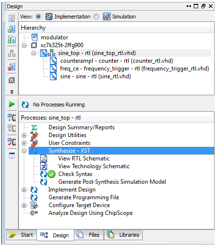
Illustration 6.2: Synthesize – XST command
6.5.3 Synthesis Report
After synthesis completes, you can view the reports, and open, analyze, and use the synthesis design. Synthesis Report contains the results from the synthesis run, including area and timing estimation. To view Synthesis Report:
- In the Project Navigator, select Project → Design Summary/Reports option from the main menu, see Illustration 6.3
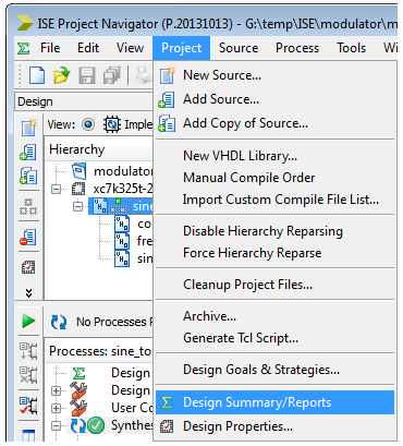
Illustration 6.3: Design Summary/Reports option
- In the Design Summary (Synthesized) window, select Detailed Reports → Synthesis Report option, see Illustration 6.4
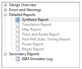
Illustration 6.4: Detailed Reports → Synthesis Report option
In the Synthesis Report you will find:
1) Synthesis Options Summary
2) HDL Parsing
3) HDL Elaboration
4) HDL Synthesis
4.1) HDL Synthesis Report
5) Advanced HDL Synthesis
5.1) Advanced HDL Synthesis Report
6) Low Level Synthesis
7) Partition Report
8) Design Summary
8.1) Primitive and Black Box Usage
8.2) Device Utilization Summary
8.3) Partition Resource Summary
8.4) Timing Report
8.4.1) Clock Information
8.4.2) Asynchronous Control Signals Information
8.4.3) Timing Summary
8.4.4) Timing Details
8.4.5) Cross Clock Domains Report
1) Synthesis Options Summary – summarized the parameters and options used for the current synthesis run, see Illustration 6.5. Changes to these options can be made by right-clicking on the Synthesize – XST process in the Project Navigator, Processes window and selecting Process Properties option.
=========================================================================
* Synthesis Options Summary *
=========================================================================
---- Source Parameters
Input File Name : "sine_top.prj"
Ignore Synthesis Constraint File : NO
---- Target Parameters
Output File Name : "sine_top"
Output Format : NGC
Target Device : xc7k325t-2-ffg900
---- Source Options
Top Module Name : sine_top
Automatic FSM Extraction : YES
FSM Encoding Algorithm : Auto
Safe Implementation : No
FSM Style : LUT
RAM Extraction : Yes
RAM Style : Auto
ROM Extraction : Yes
Shift Register Extraction : YES
ROM Style : Auto
Resource Sharing : YES
Asynchronous To Synchronous : NO
Shift Register Minimum Size : 2
Use DSP Block : Auto
Automatic Register Balancing : No
---- Target Options
LUT Combining : Auto
Reduce Control Sets : Auto
Add IO Buffers : YES
Global Maximum Fanout : 100000
Add Generic Clock Buffer(BUFG) : 32
Register Duplication : YES
Optimize Instantiated Primitives : NO
Use Clock Enable : Auto
Use Synchronous Set : Auto
Use Synchronous Reset : Auto
Pack IO Registers into IOBs : Auto
Equivalent register Removal : YES
---- General Options
Optimization Goal : Speed
Optimization Effort : 1
Power Reduction : NO
Keep Hierarchy : No
Netlist Hierarchy : As_Optimized
RTL Output : Yes
Global Optimization : AllClockNets
Read Cores : YES
Write Timing Constraints : NO
Cross Clock Analysis : NO
Hierarchy Separator : /
Bus Delimiter : <>
Case Specifier : Maintain
Slice Utilization Ratio : 100
BRAM Utilization Ratio : 100
DSP48 Utilization Ratio : 100
Auto BRAM Packing : NO
Slice Utilization Ratio Delta : 5
=========================================================================
Illustration 6.5: Synthesis Options Summary
2), 3) HDL Parsing and HDL Elaboration – during HDL parsing and elaboration, XST parses the VHDL and Verilog files that make up the synthesis project, interprets the content of those files, recognizes the design hierarchy, flags HDL coding mistakes, points out potential problems such as simulation mismatches between post-synthesis and HDL and potential multi-source situations. If problems occur at later stages of synthesis, the HDL parsing and elaboration sections may reveal the root cause of the problems.
=========================================================================
* HDL Parsing *
=========================================================================
Parsing VHDL file "G:\temp\ISE\Sources\modulator_pkg.vhd" into library work
Parsing package <modulator_pkg>.
Parsing package body <modulator_pkg>.
Parsing VHDL file "G:\temp\ISE\Sources\sine_rtl.vhd" into library work
Parsing entity <sine>.
Parsing architecture <rtl> of entity <sine>.
Parsing VHDL file "G:\temp\ISE\Sources\frequency_trigger_rtl.vhd" into library work
Parsing entity <frequency_trigger>.
Parsing architecture <rtl> of entity <frequency_trigger>.
Parsing VHDL file "G:\temp\ISE\Sources\counter_rtl.vhd" into library work
Parsing entity <counter>.
Parsing architecture <rtl> of entity <counter>.
Parsing VHDL file "G:\temp\ISE\Sources\sine_top_rtl.vhd" into library work
Parsing entity <sine_top>.
Parsing architecture <rtl> of entity <sine_top>.
=========================================================================
* HDL Elaboration *
=========================================================================
Elaborating entity <sine_top> (architecture <rtl>) with generics from library <work>.
Elaborating entity <counter> (architecture <rtl>) with generics from library <work>.
Elaborating entity <frequency_trigger> (architecture <rtl>) with generics from library <work>.
INFO:HDLCompiler:679 - "G:\temp\ISE\Sources\frequency_trigger_rtl.vhd" Line 81. Case statement is complete. others clause is never selected
Elaborating entity <sine> (architecture <rtl>) with generics from library <work>.
=========================================================================
Illustration 6.6: HDL Parsing and HDL Elaboration
4) HDL Synthesis – during HDL Synthesis XST attempts to recognize basic macros for which a technology-specific implementation might later be possible. These basic macros include: registers, adders, multipliers. During HDL Synthesis XST looks for Finite State Machine (FSM) descriptions on a block by block basis and XST issues the HDL Synthesis Report, which provides statistics on inferred macros.
=========================================================================
* HDL Synthesis *
=========================================================================
Synthesizing Unit <sine_top>.
Related source file is "G:\temp\ISE\Sources\sine_top_rtl.vhd".
cntampl_value_g = 255
depth_g = 8
width_g = 12
div_factor_freqhigh_g = 57344
div_factor_freqlow_g = 196608
Summary:
no macro.
Unit <sine_top> synthesized.
Synthesizing Unit <counter>.
Related source file is "G:\temp\ISE\Sources\counter_rtl.vhd".
cnt_value_g = 255
depth_g = 8
Found 8-bit register for signal <cnt_out_s>.
Found 8-bit adder for signal <cnt_out_s[7]_GND_8_o_add_1_OUT> created at line 60.
Summary:
inferred 1 Adder/Subtractor(s).
inferred 8 D-type flip-flop(s).
Unit <counter> synthesized.
Synthesizing Unit <frequency_trigger>.
Related source file is "G:\temp\ISE\Sources\frequency_trigger_rtl.vhd".
div_factor_freqhigh_g = 57344
div_factor_freqlow_g = 196608
Found 1-bit register for signal <freq_trig>.
Found 1-bit register for signal <sw0_jmp>.
Found 32-bit register for signal <freq_cnt_s>.
Found 32-bit adder for signal <freq_cnt_s[31]_GND_9_o_add_0_OUT> created at line 56.
Summary:
inferred 1 Adder/Subtractor(s).
inferred 34 D-type flip-flop(s).
inferred 1 Multiplexer(s).
Unit <frequency_trigger> synthesized.
Synthesizing Unit <sine>.
Related source file is "G:\temp\ISE\Sources\sine_rtl.vhd".
depth_g = 8
width_g = 12
Found 12-bit register for signal <sine_s>.
Found 8-bit register for signal <ampl_cnt_s>.
Found 256x12-bit Read Only RAM for signal <ampl_cnt_s[7]_GND_10_o_wide_mux_0_OUT>
Summary:
inferred 1 RAM(s).
inferred 20 D-type flip-flop(s).
Unit <sine> synthesized.
=========================================================================
HDL Synthesis Report
Macro Statistics
# RAMs : 1
256x12-bit single-port Read Only RAM : 1
# Adders/Subtractors : 2
32-bit adder : 1
8-bit adder : 1
# Registers : 6
1-bit register : 2
12-bit register : 1
32-bit register : 1
8-bit register : 2
# Multiplexers : 1
1-bit 2-to-1 multiplexer : 1
Illustration 6.7: HDL Synthesis and HDL Synthesis Report
5) Advanced HDL Synthesis - in this section, XST attempts to combine basic macros inferred during HDL Synthesis into larger macro blocks. The macro blocks include: counters, pipelined multipliers, multiply-accumulate functions. XST reports on the selected encoding scheme for each inferred Finite State Machine (FSM). The Advanced HDL Synthesis Report summarized the recognized macros in the overall design. The recognized macros are sorted by macro type.
=========================================================================
* Advanced HDL Synthesis *
=========================================================================
Synthesizing (advanced) Unit <counter>.
The following registers are absorbed into counter <cnt_out_s>: 1 register on signal <cnt_out_s>.
Unit <counter> synthesized (advanced).
Synthesizing (advanced) Unit <frequency_trigger>.
The following registers are absorbed into counter <freq_cnt_s>: 1 register on signal <freq_cnt_s>.
Unit <frequency_trigger> synthesized (advanced).
Synthesizing (advanced) Unit <sine>.
INFO:Xst:3226 - The RAM <Mram_ampl_cnt_s[7]_GND_10_o_wide_mux_0_OUT> will be implemented as a BLOCK RAM, absorbing the following register(s): <sine_s>
-----------------------------------------------------------------------
| ram_type | Block | |
-----------------------------------------------------------------------
| Port A |
| aspect ratio | 256-word x 12-bit | |
| mode | write-first | |
| clkA | connected to signal <clk_in> | rise |
| weA | connected to signal <GND> | high |
| addrA | connected to signal <ampl_cnt_s> | |
| diA | connected to signal <GND> | |
| doA | connected to signal <sine_s> | |
-----------------------------------------------------------------------
| optimization | speed | |
-----------------------------------------------------------------------
Unit <sine> synthesized (advanced).
=========================================================================
Advanced HDL Synthesis Report
Macro Statistics
# RAMs : 1
256x12-bit single-port block Read Only RAM : 1
# Counters : 2
32-bit up counter : 1
8-bit up counter : 1
# Registers : 10
Flip-Flops : 10
Illustration 6.8: Advanced HDL Synthesis and Advanced HDL Synthesis Report
6) Low Level Synthesis – this section displays information about XST low-level optimizations, including: removal of equivalent flip-flops, optimization of constant flip-flops, register replication, see Illustration 6.9
=========================================================================
* Low Level Synthesis *
=========================================================================
Optimizing unit <sine> ...
Optimizing unit <sine_top> ...
Optimizing unit <frequency_trigger> ...
Mapping all equations...
Building and optimizing final netlist ...
Found area constraint ratio of 100 (+ 5) on block sine_top, actual ratio is 0.
Final Macro Processing ...
=========================================================================
Final Register Report
Macro Statistics
# Registers : 50
Flip-Flops : 50
Illustration 6.9: Low Level Synthesis
7) Partition Report – displays information about the design partitions, see Illustration 6.10
=========================================================================
* Partition Report *
=========================================================================
Partition Implementation Status
-------------------------------
No Partitions were found in this design.
-------------------------------
Illustration 6.10: Partition Report
8) Design Summary:
8.1) Primitive and Black Box Usage – this subsection displays usage statistics for: device primitives and identified black boxes. The primitives are classified in the following groups: BELs, all basic logical primitives (such as LUT, MUXCY, XORCY, MUXF5, MUXF6), flip-flops and latches, block and distributed RAM, shift register primitives, tristate buffers, clock buffers, I/O buffers, other logical, more complex, primitives (such as AND2 and OR2), other primitives, see Illustration 6.11
=========================================================================
* Design Summary *
=========================================================================
Top Level Output File Name : sine_top.ngc
Primitive and Black Box Usage:
------------------------------
# BELS : 163
# GND : 1
# INV : 2
# LUT1 : 38
# LUT2 : 32
# LUT4 : 2
# LUT5 : 1
# LUT6 : 8
# MUXCY : 38
# VCC : 1
# XORCY : 40
# FlipFlops/Latches : 50
# FD : 42
# FDRE : 8
# RAMS : 1
# RAMB18E1 : 1
# Clock Buffers : 1
# BUFGP : 1
# IO Buffers : 13
# IBUF : 1
# OBUF : 12
Illustration 6.11: Primitive and Black Box Usage
8.2) Device Utilization Summary – displays device utilization estimates for: slice logic utilization, slice logic distribution, number of flip-flops, I/O utilization, number of block RAM components, number of DSP blocks, see Illustration 6.12. XST generates a similar report when you later run MAP.
Device utilization summary:
---------------------------
Selected Device : 7k325tffg900-2
Slice Logic Utilization:
Number of Slice Registers: 50 out of 407600 0%
Number of Slice LUTs: 83 out of 203800 0%
Number used as Logic: 83 out of 203800 0%
Slice Logic Distribution:
Number of LUT Flip Flop pairs used: 92
Number with an unused Flip Flop: 42 out of 92 45%
Number with an unused LUT: 9 out of 92 9%
Number of fully used LUT-FF pairs: 41 out of 92 44%
Number of unique control sets: 2
IO Utilization:
Number of IOs: 14
Number of bonded IOBs: 14 out of 500 2%
Specific Feature Utilization:
Number of Block RAM/FIFO: 1 out of 445 0%
Number using Block RAM only: 1
Number of BUFG/BUFGCTRLs: 1 out of 32 3%
Illustration 6.12: Device Utilization Summary
8.3) Partition Resource Summary – if partitions have been defined, the Partition Resources Summary subsection displays information similar to the Device Utilization Summary on a partition-by-partition basis.
Partition Resource Summary:
---------------------------
No Partitions were found in this design.
Illustration 6.13: Partition Resource Summary
8.4) Timing Report – this subsection displays timing estimates to help you: determine whether the design meets performance and timing requirements, and locate bottlenecks if performance and timing requirements are not met.
8.4.1) Clock Information - gives information about the number of clocks in the design, how each clock is buffered and their respective fanouts, see Illustration 6.13.
=========================================================================
Timing Report
NOTE: THESE TIMING NUMBERS ARE ONLY A SYNTHESIS ESTIMATE.
FOR ACCURATE TIMING INFORMATION PLEASE REFER TO THE TRACE REPORT
GENERATED AFTER PLACE-and-ROUTE.
Clock Information:
------------------
-----------------------------------+------------------------+-------+
Clock Signal | Clock buffer(FF name) | Load |
-----------------------------------+------------------------+-------+
clk_in | BUFGP | 51 |
-----------------------------------+------------------------+-------+
Illustration 6.13: Timing Report and Clock Information
8.4.2) Asynchronous Control Signals Information – displays information about the number of asynchronous set/reset signals, how each signal is buffered and their respective fanouts, see Illustration 6.14.
Asynchronous Control Signals Information:
----------------------------------------
-----------------------------------+------------------------------------------------------+-------+
Control Signal | Buffer(FF name) | Load |
-----------------------------------+------------------------------------------------------+-------+
N0(XST_GND:G) | NONE(sine_Mram_ampl_cnt_s[7]_GND_10_o_wide_mux_0_OUT)| 2 |
-----------------------------------+------------------------------------------------------+-------+
Illustration 6.14. Asynchronous Control Signals Information
8.4.3) Timing Summary – shows timing information for all four possible clock domains of a netlist: minimum clock period, minimum input arrival time before clock, maximum output required time after clock and maximum combinational path delay, see Illustration 6.15.
8.4.4) Timing Details – displays information about the most critical path in each clock region. The information includes start and end point, maximum delay, levels of logic, detailed breakdown of the path into individual net and component delays, information on net fanouts, distribution between routing and logic, see Illustration 6.15.
Timing Summary:
---------------
Speed Grade: -2
Minimum period: 2.380ns (Maximum Frequency: 420.156MHz)
Minimum input arrival time before clock: 1.786ns
Maximum output required time after clock: 2.139ns
Maximum combinational path delay: No path found
Timing Details:
---------------
All values displayed in nanoseconds (ns)
=========================================================================
Timing constraint: Default period analysis for Clock 'clk_in'
Clock period: 2.380ns (frequency: 420.156MHz)
Total number of paths / destination ports: 1748 / 73
-------------------------------------------------------------------------
Delay: 2.380ns (Levels of Logic = 4)
Source: freq_ce/freq_cnt_s_12 (FF)
Destination: freq_ce/freq_cnt_s_31 (FF)
Source Clock: clk_in rising
Destination Clock: clk_in rising
Data Path: freq_ce/freq_cnt_s_12 to freq_ce/freq_cnt_s_31
Gate Net
Cell:in->out fanout Delay Delay Logical Name (Net Name)
---------------------------------------- ------------
FD:C->Q 2 0.236 0.608 freq_ce/freq_cnt_s_12 (freq_ce/freq_cnt_s_12)
LUT5:I0->O 1 0.043 0.522 freq_ce/GND_9_o_GND_9_o_MUX_44_o2 (freq_ce/GND_9_o_GND_9_o_MUX_44_o2)
LUT6:I2->O 3 0.043 0.362 freq_ce/GND_9_o_GND_9_o_MUX_44_o5 (freq_ce/GND_9_o_GND_9_o_MUX_44_o5)
LUT6:I5->O 31 0.043 0.480 freq_ce/Mcount_freq_cnt_s_val321 (freq_ce/Mcount_freq_cnt_s_val)
LUT2:I1->O 1 0.043 0.000 freq_ce/freq_cnt_s_31_rstpot (freq_ce/freq_cnt_s_31_rstpot)
FD:D -0.000 freq_ce/freq_cnt_s_31
----------------------------------------
Total 2.380ns (0.408ns logic, 1.972ns route)
(17.1% logic, 82.9% route)
=========================================================================
Timing constraint: Default OFFSET IN BEFORE for Clock 'clk_in'
Total number of paths / destination ports: 66 / 34
-------------------------------------------------------------------------
Offset: 1.786ns (Levels of Logic = 5)
Source: sw0 (PAD)
Destination: freq_ce/freq_cnt_s_31 (FF)
Destination Clock: clk_in rising
Data Path: sw0 to freq_ce/freq_cnt_s_31
Gate Net
Cell:in->out fanout Delay Delay Logical Name (Net Name)
---------------------------------------- ------------
IBUF:I->O 4 0.000 0.367 sw0_IBUF (sw0_IBUF)
LUT6:I5->O 1 0.043 0.405 freq_ce/GND_9_o_GND_9_o_MUX_44_o3 (freq_ce/GND_9_o_GND_9_o_MUX_44_o3)
LUT6:I4->O 3 0.043 0.362 freq_ce/GND_9_o_GND_9_o_MUX_44_o5 (freq_ce/GND_9_o_GND_9_o_MUX_44_o5)
LUT6:I5->O 31 0.043 0.480 freq_ce/Mcount_freq_cnt_s_val321 (freq_ce/Mcount_freq_cnt_s_val)
LUT2:I1->O 1 0.043 0.000 freq_ce/freq_cnt_s_31_rstpot (freq_ce/freq_cnt_s_31_rstpot)
FD:D -0.000 freq_ce/freq_cnt_s_31
----------------------------------------
Total 1.786ns (0.172ns logic, 1.614ns route)
(9.6% logic, 90.4% route)
=========================================================================
Timing constraint: Default OFFSET OUT AFTER for Clock 'clk_in'
Total number of paths / destination ports: 12 / 12
-------------------------------------------------------------------------
Offset: 2.139ns (Levels of Logic = 1)
Source: sine_Mram_ampl_cnt_s[7]_GND_10_o_wide_mux_0_OUT (RAM)
Destination: sine_out<11> (PAD)
Source Clock: clk_in rising
Data Path: sine_Mram_ampl_cnt_s[7]_GND_10_o_wide_mux_0_OUT to sine_out<11>
Gate Net
Cell:in->out fanout Delay Delay Logical Name (Net Name)
---------------------------------------- ------------
RAMB18E1:CLKARDCLK->DOADO11 1 1.800 0.339 sine_Mram_ampl_cnt_s[7]_GND_10_o_wide_mux_0_OUT (sine_out_11_OBUF)
OBUF:I->O 0.000 sine_out_11_OBUF (sine_out<11>)
----------------------------------------
Total 2.139ns (1.800ns logic, 0.339ns route)
(84.1% logic, 15.9% route)
=========================================================================
Illustration 6.15: Timing Summary and Timing Details
8.4.5) Cross Clock Domain Report – this subsection reports Clock Domain Crossing (CDC) path, is included by default, follows the Timing Details section, is available whether or not XST has performed cross clock domain optimization, is available whether or not you have specified timing constraints in an XST Constraint File (XCF). You don't need to enable Cross Clock Analyzer to obtain cross clock domain timing information. Use Cross Clock Analyzer only in order to achieve timing optimizations across clock domains.
Cross Clock Domains Report:
--------------------------
Clock to Setup on destination clock clk_in
---------------+---------+---------+---------+---------+
| Src:Rise| Src:Fall| Src:Rise| Src:Fall|
Source Clock |Dest:Rise|Dest:Rise|Dest:Fall|Dest:Fall|
---------------+---------+---------+---------+---------+
clk_in | 2.380| | | |
---------------+---------+---------+---------+---------+
Illustration 6.16: Cross Clock Domains Report
6.5.4 RTL and Technology Schematic Viewers
RTL and Technology Schematic Viewers allow you to view a schematic representation of your synthesized netlist. These viewers help you to:
-
Analyse how components were inferred
-
Analyse timing paths
-
Identify issues and improve your design early in the design process
RTL Schematic Viewer
RTL Schematic viewer allows you to view a schematic representation of the design in terms of generic symbols that are independent of the targeted Xilinx device, for example, in terms of adders, multipliers, counters, AND gates, and OR gates.
To use the RTL Schematic viewer, follow these steps:
- In the Hierarchy window, select the synthesizable module (sine_top – rtl). In the Processes window expand Synthesize - XST option and double-click on the View RTL Schematic command, see Illustration 6.17
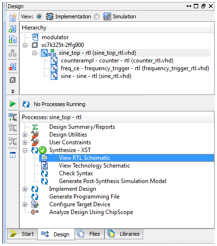
Illustration 6.17: View RTL Schematic command
-
In the Set RTL/Tech Viewer Startup Mode dialog box, select Start with the Explorer Wizard option and click OK, see Illustration 6.18
As it is explained in the Set RTL/Tech Viewer Startup Mode dialog box, in this mode, the Explorer Wizard is the initial screen and allows you to select the elements that you want to see on the initial schematic, see Illustration 6.19.
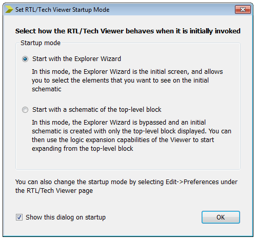
Illustration 6.18: Set RTL/Tech Viewer Startup Mode dialog box
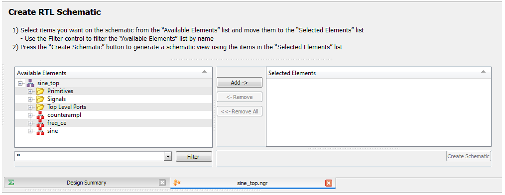
Illustration 6.19: Create RTL Schematic window
- To create a detailed RTL Schematic view, you have to select items you want on the schematic from the Available Elements list (sine_top in our case) and add them to the Selected Elements list, see Illustration 6.20
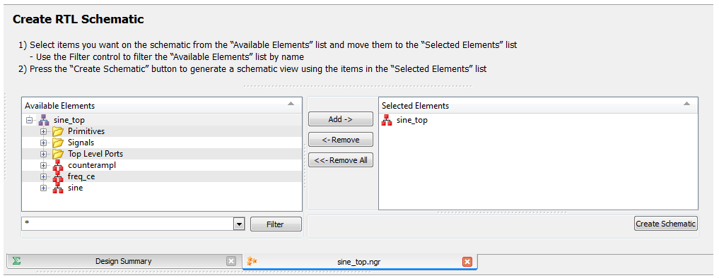
Illustration 6.20: Create RTL Schematic window with selected sine_top element
- Press the Create Schematic button to generate a schematic view using the items in the Selected Elements list, see Illustration 6.21 and 6.22
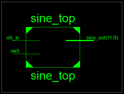
Illustration 6.21: RTL Schematic View of the Digital Sine Top module
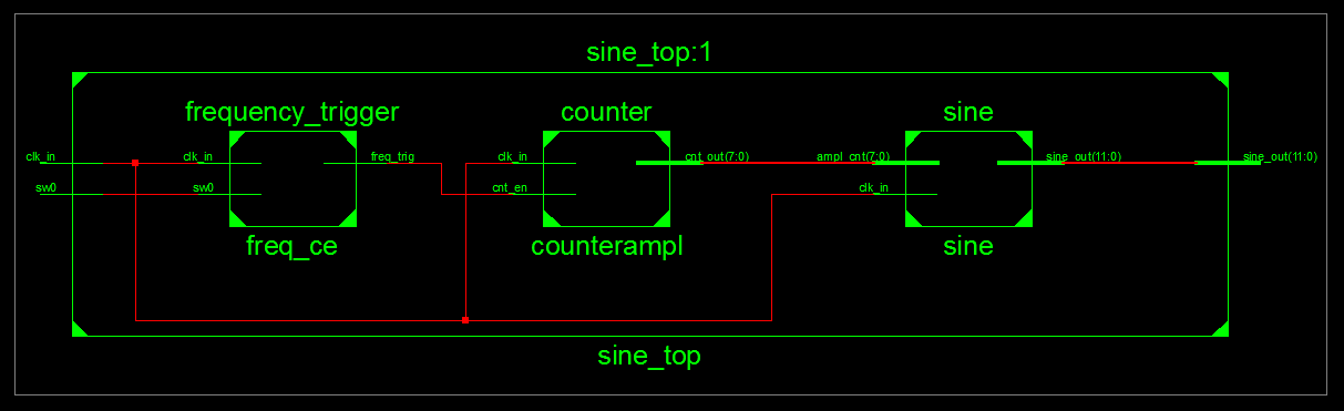
Illustration 6.22: Detailed RTL Schematic View of the Digital Sine Top module
- Optional: If you want a more detailed logical view of your design, double-click on the schematic part to zoom-in, see Illustration 6.22
- Optional: If you want to return to the Top-Schematic, you should click on the green arrow on the left side of your schematic window
6.5.5 View Technology Schematic
Technology Schematic viewer allows you to view a schematic representation of the design in terms of logic elements optimized to the target Xilinx device or "technology," for example, in terms of LUTs, carry logic, I/O buffers, and other technology-specific components.
To use the Technology Schematic Viewer:
- In the Hierarchy window, select the synthesizable module (sine_top – rtl). In the Processes window expand Synthesize - XST option and double-click on the View Technology Schematic command, see Illustration 6.23
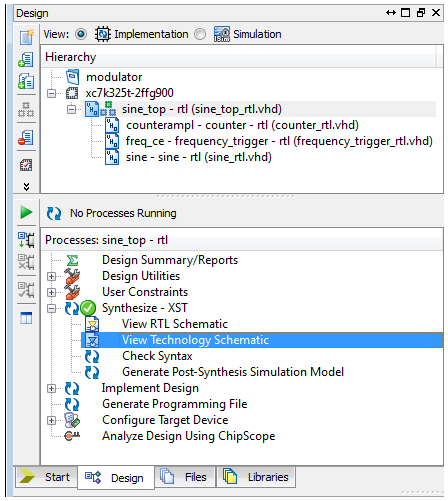
Illustration 6.23: View technology Schematic command
- Repeat steps 2-6 from the previous Sub-chapter 6.5.4 RTL and Technology Schematic Viewers and you will create detailed Technology Schematic view of your design, see Illustration 6.24
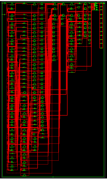
Illustration 6.24: Detailed Technology Schematic View of the Digital Sine Top module
Note: If you want to go more detail in the technology schematic view of you design, please press and hold Ctrl button on your keyboard and scroll-in with your mouse.
6.5.6 Check Syntax
The Check Syntax process checks the syntax of the selected source file prior to generating a netlist of the design by synthesis or compile, or prior to running a simulation with ISim.
To use Check Syntax process:
- In the Hierarchy window, select the synthesizable module (sine_top – rtl). In the Processes window expand Synthesize - XST option and double-click on the Check Syntax command, see Illustration 6.25
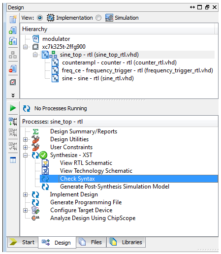
Illustration 6.25: Check Syntax command
Note: The Check Syntax process is also explained in the Sub-chapter 2.3.1 Creating a Module Using an Text Editor– step 8.
6.5.7 Generate Post-Synthesis Simulation Model
You can generate a simulation model after synthesizing your design. For this process, NetGen converts the synthesis output (NGC) to a simulation model (a structural UNISIM-based VHDL or Verilog file). The simulation model can be used to verify that the functionality is correct after synthesis by running a post-synthesis simulation in your simulator.
To Generate Post-Synthesis Simulation Model, follow these steps:
- In the Processes window, expand Synthesize – XST option
- Right-click on the Generate Post-Synthesis Simulation Model and choose Process Properties... option
- In the Process Properties – Simulation Model Properties window, write in the “Rename Top Level Architecture To” filed rtl, and click OK, see Illustration 6.26
Note: Verify that the Advanced Property Display Level is enabled in the Process Properties window.
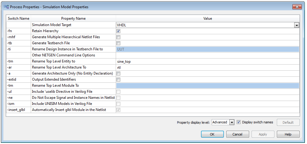
Illustration 6.26: Process Properties – Simulation Model Properties window
- At the end, double-click on the Generate Post-Synthesis Simulation Model, see Illustration 6.27
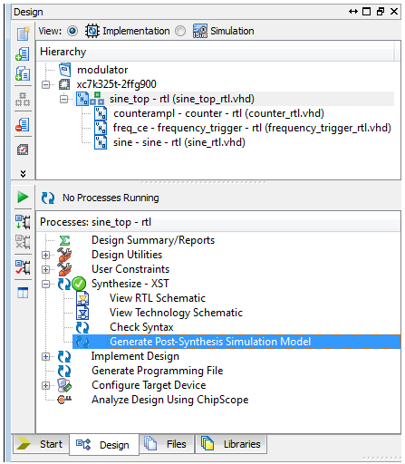
Illustration 6.18: Generate Post-Synthesis Simulation Model command